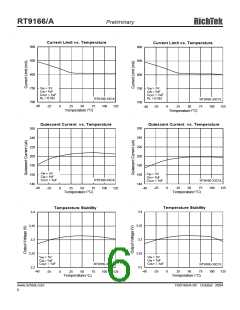
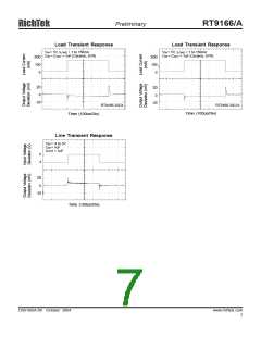
Preliminary
RT9166/A
Thermal Considerations
It should be noted that stability problems have been seen
in applications where “ vias” to an internal ground plane
were used at the ground points of the device and the
input and output capacitors. This was caused by varying
ground potentials at these nodes resulting from current
flowing through the ground plane. Using a single point
ground technique for the regulator and it’ s capacitors fixed
the problem. Since high current flows through the traces
going into VIN and coming from VOUT, Kelvin connect the
capacitor leads to these pins so there is no voltage drop
in series with the input and output capacitors.
The RT9166/A series can deliver a current of up to 300/
600mAover the full operating junction temp-erature range.
However, the maximum output current must be derated
at higher ambient temperature to ensure the junction
temperature does not exceed 125°C. With all possible
conditions, the junction temperature must be within the
range specified under operating conditions. Power
dissipation can be calculated based on the output current
and the voltage drop across regulator.
PD = (VIN - VOUT) IOUT + VIN IGND
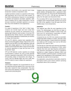
Optimum performance can only be achieved when the
device is mounted on a PC board according to the diagram
below:
The final operating junction temperature for any set of
conditions can be estimated by the following thermal
equation:
PD (MAX) = ( TJ (MAX) - TA ) / θJA
Where TJ(MAX) is the maximum junction temperature of
the die (125°C) and TA is the maximum ambient
temperature. The junction to ambient thermal resistance
(θJA) for SOT-23 package at recomm-ended minimum
footprint is 250°C/W, 175°C/W for SOT-89 package and
135°C/W for SOT-223 package (θJA is layout dependent).
Visit our website in which “Recommended Footprints for
Soldering Surface Mount Packages” for detail.
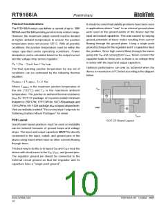
V
IN
GND
V
OUT
PCB Layout
SOT-23 Board Layout
Good board layout practices must be used or instability
can be induced because of ground loops and voltage
drops. The input and output capacitors MUST be directly
connected to the input, output, and ground pins of the
device using traces which have no other currents flowing
through them.
The best way to do this is to layout CIN and COUT near the
device with short traces to the VIN, VOUT, and ground pins.
The regulator ground pin should be connected to the
external circuit ground so that the regulator and its
capacitors have a “single point ground”.
www.richtek.com
10
DS9166/A-09 October 2004

 ETC [ ETC ]