i
sharp
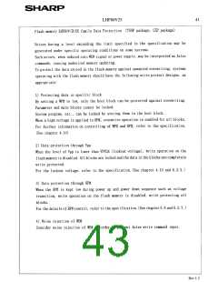
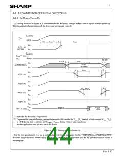
A-1 RECOMMENDED OPERATING CONDITIONS
A-1.1 At Device Power-Up
AC timing illustrated in Figure A-1 is recommended for the supply voltages and the control signals at device power-up.
If the timing in the figure is ignored, the device may not operate correctly.
VCC(min)
VCC
GND
*1
tVR
tR
t2VPH
tPHQV
VIH
(P)
RP#
(RST#)
VIL
VCCWH1/2
(VPPH1/2)
*2
(V)
VCCW
(VPP)
GND
tR or tF
tR or tF
tAVQV
VIH
Valid
Address
ADDRESS (A)
VIL
tR
tF
tELQV
VIH
VIL
VIH
VIL
VIH
VIL
VIH
(E)
CE#
(W)
WE#
tR
tF
tGLQV
(G)
OE#
(S)
WP#
VIL
VOH
High Z
Valid
Output
DATA
(D/Q)
V
OL
*1 t5VPH for the device in 5V operations.
*2 To prevent the unwanted writes, system designers should consider the VCCW (VPP) switch, which connects VCCW (VPP)
to GND during read operations and VCCWH1/2 (VPPH1/2) during write or erase operations.
See the application note AP-007-SW-E for details.
Figure A-1. AC Timing at Device Power-Up
For the AC specifications t , t , t in the figure, refer to the next page. See the “ELECTRICAL SPECIFICATIONS“
VR
R
F
described in specifications for the supply voltage range, the operating temperature and the AC specifications not shown in
the next page.
Rev. 1.10

 ETC [ ETC ]