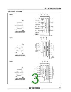
HCC/HCF4054B/55B/56B
ABSOLUTE MAXIMUM RATINGS
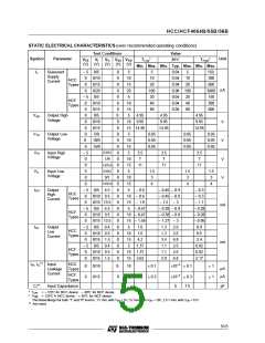
Symbol
Parameter
Value
Unit
VDD
*
Supply Voltage : HCC Types
HCF Types
– 0.5 to + 20
– 0.5 to + 18
V
V
Vi
II
Input Voltage
– 0.5 to VDD + 0.5
V
DC Input Current (any one input)
± 10
mA
mW
Pt ot
Total Power Dissipation (per package)
Dissipation per Output Transistor
200
for Top = Full Package-temperature Range
100
mW
To p
Tstg
Operating Temperature : HCC Types
HCF Types
– 55 to + 125
– 40 to + 85
°C
°C
Storage Temperature
– 65 to + 150
°C
Stresses above those listed under ”Absolute Maximum Ratings” may cause permanent damage to the device. This is a stress rating only
and functional operation of the device at these or any other conditions above those indicated in the operational sections of this specification
is not implied. Exposure to absolute maximum rating conditions for external periods may affect device reliability.
*
All voltage values are referred to VSS pin voltage.
RECOMMENDED OPERATING CONDITIONS
Symbol
Parameter
Supply Voltage : HCC Types
HCF Types
Value
Unit
VDD
3 to 18
3 to 15
V
V
VI
Input Voltage
0 to VDD
V
Top
Operating Temperature : HCC Types
HCF Types
– 55 to 125
– 40 to 85
°C
°C
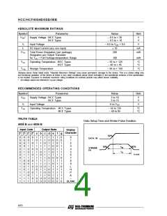
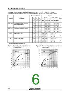
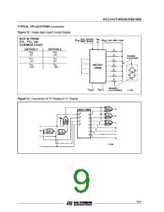
TRUTH TABLE
Data Setup Time and Strobe Pulse Duration.
4055 B and 4056 B
Input Code
23 22 21 20
Output State
Display
Character
a
b
c
d
e
f
g
0
0
0
0
0
0
0
0
1
1
1
1
1
1
1
1
0
0
0
0
1
1
1
1
0
0
0
0
1
1
1
1
0
0
1
1
0
0
1
1
0
0
1
1
0
0
1
1
0
1
0
1
0
1
0
1
0
1
0
1
0
1
0
1
1
0
1
1
0
1
1
1
1
1
0
0
1
1
0
0
1
1
1
1
1
0
0
1
1
1
0
1
1
1
0
0
1
1
0
1
1
1
1
1
1
1
0
1
0
1
0
0
1
0
1
1
0
1
1
0
1
1
1
0
0
0
0
0
1
0
1
0
0
0
1
0
1
0
1
1
1
1
0
0
1
0
0
0
1
1
1
0
1
1
1
1
1
1
0
0
0
0
1
1
1
1
1
0
1
1
0
1
1
1
1
0
0
1
2
3
4
5
6
7
8
9
L
H
P
A
–
BLANK
4/15

 ETC [ ETC ]