I TECHNICAL NOTES
When using these ICs, consider the following points:
Phase Compensation
In these ICs, phase compensation is made for securing stable operation even if the load current is varied. For this purpose, be
sure to use a 2.2µF or more capacitor COUT with good frequency characteristics and ESR (Equivalent Series Resistance).
(Note: When the additional ceramic capacitors are connected to the Output Pin with Output capacitor for phase compensation,
the operation might be unstable. Because of this, test these ICs with as same external components as ones to be used on the
PCB.) If you use a ceramic capacitor to the output pin, add as much as 1Ω resistor to compensate ESR value of the capacitor.
As for the input, as much as 1.0µF ceramic capacitor is also recommended.
PCB Layout
Make VDD and GND line sufficient. When the impedance of these is high, it would be a cause of picking up the noise or
unstable operation. Connect a capacitor with as much as 1.0µF capacitor between VDD and GND pin as close as possible.
Set external components, especially output capacitor as close as possible to the ICs and make wiring shortest.
I TEST CIRCUITS
*1
VDD
OUT
IN
V
OUT
I
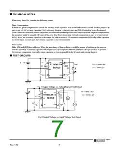
:*1 C1 = Tantal1.0µF
C2 = Tantal2.2µF
R1160XXX1X
SERIES
C1
A
C2
GND
ECO4
CE
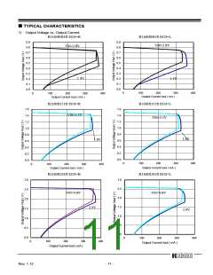
Fig.1 Output Voltage vs. Output Current Test Circuit
C1 = Tantal 1.0µF
C2 = Tantal 2.2µF
VDD
OUT
R1160XXX1X
C1
C2
GND SERIES
CE
ECO4
V
Fig.2 Output Voltage vs. Input Voltage Test Circuit
Rev. 1.12
- 7 -

 ETC [ ETC ]