PIC16C5X
4.7
Indirect Data Addressing; INDF and
FSR Registers
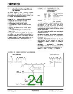
EXAMPLE 4-2: HOW TO CLEAR RAM
USING INDIRECT
ADDRESSING
The INDF register is not
a physical register.
movlw 0x10
;initialize pointer
Addressing INDF actually addresses the register
whose address is contained in the FSR register (FSR
is a pointer). This is indirect addressing.
movwf FSR
; to RAM
;clear INDF register
NEXT
clrf
incf
INDF
FSR,F ;inc pointer
btfsc FSR,4 ;all done?
goto
NEXT
;NO, clear next
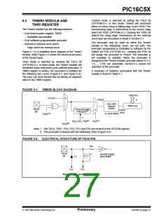
EXAMPLE 4-1: INDIRECT ADDRESSING
• Register file 05 contains the value 10h
• Register file 06 contains the value 0Ah
• Load the value 05 into the FSR register
• A read of the INDF register will return the value
of 10h
• Increment the value of the FSR register by one
(FSR = 06)
• A read of the INDR register now will return the
value of 0Ah.
CONTINUE
:
;YES, continue
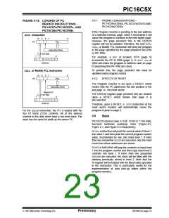
The FSR is either a 5-bit (PIC16C52, PIC16C54s,
PIC16CR54s, PIC16C55s), 6-bit (PIC16C56s,
PIC16CR56s), or 7-bit (PIC16C57s, PIC16CR57s,
PIC16C58s, PIC16CR58s) wide register. It is used in
conjunction with the INDF register to indirectly address
the data memory area.
The FSR<4:0> bits are used to select data memory
addresses 00h to 1Fh.
Reading INDF itself indirectly (FSR = 0) will produce
00h. Writing to the INDF register indirectly results in a
no-operation (although STATUS bits may be affected).
PIC16C52, PIC16C54s, PIC16CR54s, PIC16C55s:
Do not use banking. FSR<6:5> are unimplemented
and read as '1's.
A simple program to clear RAM locations 10h-1Fh
using indirect addressing is shown in Example 4-2.
PIC16C56s, PIC16CR56s: FSR<6:5> are the bank
select bits and are used to select the bank to be
addressed (00= bank 0, 01= bank 1, 10= invalid, 11
= invalid).
PIC16C57s,
PIC16CR57s,
PIC16C58s,
PIC16CR58s: FSR<6:5> are the bank select bits and
are used to select the bank to be addressed (00 =
bank 0, 01= bank 1, 10= bank 2, 11= bank 3).
FIGURE 4-13: DIRECT/INDIRECT ADDRESSING
Direct Addressing
Indirect Addressing
(FSR)
4
(opcode)
0
5
(FSR)
0
6
4
5
6
location select
bank select
location select
bank
00
01
10
11
00h
Addresses map back
to addresses in Bank 0.
Data
Memory
0Fh
10h
(1)
1Fh
Bank 0
3Fh
Bank 1
5Fh
Bank 2
7Fh
Bank 3
Note 1: For register map detail see Section 4.2.
DS30453A-page 24
Preliminary
1997 Microchip Technology Inc.

 ETC [ ETC ]