IR2112
Dynamic Electrical Characteristics
V
(V , V , V ) = 15V, C = 1000 pF, T = 25°C and V = COM unless otherwise specified. The dynamic
BIAS
CC
BS DD
L
A
SS
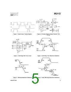
electrical characteristics are measured using the test circuit shown in Figure 3.
Symbol
Definition
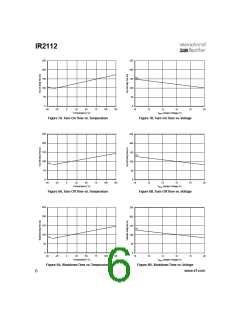
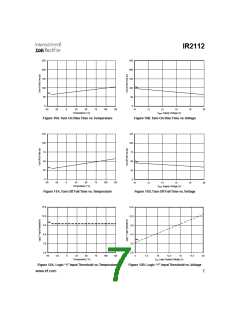
Turn-On Propagation Delay
Turn-Off Propagation Delay
Shutdown Propagation Delay
Turn-On Rise Time
Figure Min. Typ. Max. Units Test Conditions
t
on
7
—
—
—
—
—
—
125
105
105
80
180
160
160
130
65
V = 0V
S
t
off
8
V
= 600V
= 600V
S
S
t
sd
9
V
ns
t
r
10
11
—
t
f
Turn-Off Fall Time
40
MT
Delay Matching, HS & LS Turn-On/Off
—
30
Figure 5
Static Electrical Characteristics
V
(V , V , V ) = 15V, T = 25°C and V = COM unless otherwise specified. The V , V and I parameters
BIAS CC BS DD
A SS IN TH IN
are referenced to V and are applicable to all three logic input leads: HIN, LIN and SD. The V and I parameters are
SS
O
O
referenced to COM and are applicable to the respective output leads: HO or LO.
Symbol
Definition
Figure Min. Typ. Max. Units Test Conditions
V
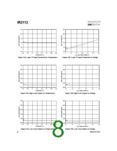
Logic “1” Input Voltage
12
13
14
15
16
17
18
19
20
9.5
—
—
—
—
—
—
—
—
—
—
6.0
100
100
50
IH
V
V
Logic “0” Input Voltage
—
IL
V
OH
High Level Output Voltage, V
- V
O
—
I
I
= 0A
= 0A
BIAS
O
mV
V
OL
Low Level Output Voltage, V
—
O
O
I
LK
Offset Supply Leakage Current
Quiescent V Supply Current
—
V = V = 600V
B S
I
25
80
2.0
20
60
V
= 0V or V
= 0V or V
= 0V or V
QBS
BS
IN
IN
IN
DD
DD
DD
I
Quiescent V
Quiescent V
Supply Current
Supply Current
180
5.0
40
V
V
QCC
CC
µA
I
QDD
DD
I
Logic “1” Input Bias Current
Logic “0” Input Bias Current
V = V
IN DD
IN+
I
IN-
21
22
—
—
1.0
9.6
V
IN
= 0V
V
V
Supply Undervoltage Positive Going
BS
7.4
8.5
BSUV+
Threshold
Supply Undervoltage Negative Going
V
V
23
24
25
26
27
7.0
7.6
7.2
200
420
8.1
8.6
8.2
250
500
9.2
9.6
9.2
—
BSUV-
BS
Threshold
V Supply Undervoltage Positive Going
CC
Threshold
V Supply Undervoltage Negative Going
CC
V
V
CCUV+
V
CCUV-
Threshold
I
Output High Short Circuit Pulsed Current
V =0V, V =V
O+
O
IN
DD
PW ≤ 10 µs
mA
I
O-
Output Low Short Circuit Pulsed Current
—
V
O
= 15V, V = 0V
IN
PW ≤ 10 µs
www.irf.com
3

 ETC [ ETC ]