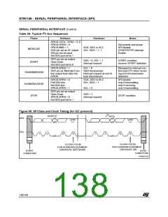
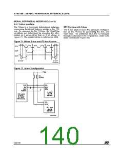
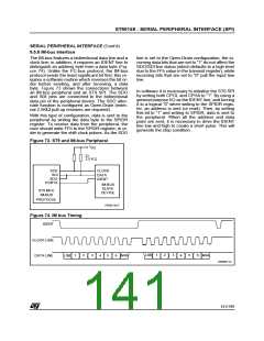
ST90158 - SERIAL PERIPHERAL INTERFACE (SPI)
SERIAL PERIPHERAL INTERFACE (Cont’d)
9.5.9 Register Description
1: Both alternate functions SCK and SDO are ena-
bled.
It is possible to have up to 3 independent SPIs in
the same device (refer to the device block dia-
gram). In this case they are named SPI0 thru
SPI2. If the device has one SPI converter it uses
the register adresses of SPI0. The register map is
the following:
Note: furthermore, SPEN (together with the BMS
bit) affects the selection of the source for interrupt
channel B0. Transmission starts when data is writ-
ten to the SPIDR Register.
2
Register
SPIn
SPI0
SPI0
SPI1
SPI1
SPI2
SPI2
Page
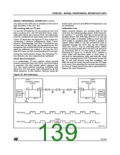
Bit 6 = BMS: S-bus/I C-bus Mode Selector.
0: Perform a re-initialisation of the SPI logic, thus
allowing recovery procedures after a RX/TX fail-
ure.
1: Enable S-bus/I C-bus arbitration, clock synchro-
nization and Start/ Stop detection (SPI used in
SPIDR R253
SPICR R254
SPIDR1 R253
SPICR1 R254
SPIDR2 R245
SPICR2 R246
0
0
7
7
7
7
2
2
an S-bus/I C-bus protocol).
Note: when the BMS bit is reset, it affects (togeth-
er with the SPEN bit) the selection of the source
for interrupt channel B0.
Note: In the register description on the following
pages, register and page numbers are given using
the example of SPI0.
Bit 5 = ARB: Arbitration flag bit.
This bit is set by hardware and can be reset by
software.
0: S-bus/I C-bus stop condition is detected.
1: Arbitration lost by the SPI in S-bus/I C-bus
SPI DATA REGISTER (SPIDR)
R253 - Read/Write
Register Page: 0
2
2
Reset Value: undefined
mode.
Note: when ARB is set automatically, the SDO pin
is set to a high value until a write instruction on
SPIDR is performed.
7
0
D7
D6
D5
D4
D3
D2
D1
D0
Bit 4 = BUSY: SPI Busy Flag.
Bit 7:0 = D[0:7]: SPI Data.
This bit is set by hardware. It allows the user to
monitor the SPI status by polling its value.
0: No transmission in progress.
This register contains the data transmitted and re-
ceived by the SPI. Data is transmitted bit 7 first,
and incoming data is received into bit 0. Transmis-
sion is started by writing to this register.
1: Transmission in progress.
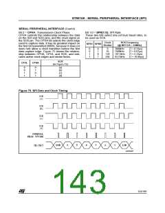
Bit 3 = CPOL: Transmission Clock Polarity.
Note: SPIDR state remains undefined until the
end of transmission of the first byte.
CPOL controls the normal or steady state value of
the clock when data is not being transferred.
Please refer to the following table and to Figure 75
to see this bit action (together with the CPHA bit).
SPI CONTROL REGISTER (SPICR)
R254 - Read/Write
Register Page: 0
Note: As the SCK line is held in a high impedance
state when the SPI is disabled (SPEN = “0”), the
Reset Value: 0000 0000 (00h)
SCK pin must be connected to V
or to V
SS
CC
through a resistor, depending on the CPOL state.
Polarity should be set during the initialisation rou-
tine, in accordance with the setting of all peripher-
als, and should not be changed during program
execution.
7
0
SPEN BMS ARB BUSY CPOL CPHA SPR1 SPR0
Bit 7 = SPEN: Serial Peripheral Enable.
0: SCK and SDO are kept tristate.
142/199
9

 ETC [ ETC ]