ST90158 - SERIAL PERIPHERAL INTERFACE (SPI)
SERIAL PERIPHERAL INTERFACE (Cont’d)
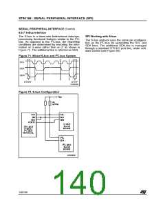
9.5.8 IM-bus Interface
The IM-bus features a bidirectional data line and a
clock line; in addition, it requires an IDENT line to
distinguish an address byte from a data byte (Fig-
line is set to the Open-Drain configuration, the in-
coming data bits that are set to “1” do not affect the
SDO/SDI line status (which defaults to a high level
due to the FFh value in the transmit register), while
incoming bits that are set to “0” pull the input line
low.
2
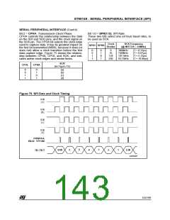
ure 74). Unlike the I C-bus protocol, the IM-bus
protocol sends the least significant bit first; this re-
quires a software routine which reverses the bit or-
der before sending, and after receiving, a data
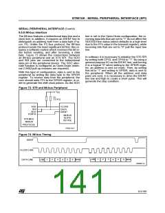
byte. Figure 73 shows the connections between
an IM-bus peripheral and an ST9 SPI. The SDO
and SDI pins are connected to the bidirectional
data pin of the peripheral device. The SDO alter-
nate function is configured as Open-Drain (exter-
nal 2.5KΩ pull-up resistors are required).
With this type of configuration, data is sent to the
peripheral by writing the data byte to the SPIDR
register. To receive data from the peripheral, the
user should write FFh to the SPIDR register, in or-
der to generate the shift clock pulses. As the SDO
In software it is necessary to initialise the ST9 SPI
by setting both CPOL and CPHA to “1”. By using a
general purpose I/O as the IDENT line, and forcing
it to a logical “0” when writing to the SPIDR regis-
ter, an address is sent (or read). Then, by setting
this bit to “1” and writing to SPIDR, data is sent to
the peripheral. When all the address and data
pairs are sent, it is necessary to drive the IDENT
line low and high to create a short pulse. This will
generate the stop condition.
Figure 73. ST9 and IM-bus Peripheral
V
DD
2x
2.5 K
SCK
SDI
CLOCK
DATA
SDO
IDENT
PORTX
IM-BUS
SLAVE
DEVICE
ST9 MCU
IM-BUS
PROTOCOL
VR001427
n
Figure 74. IM bus Timing
IDENT
CLOCK LINE
LSB
2
3
6
MSB
2
MSB
1
5
3
DATA LINE
LSB
1
4
5
6
4
VR000172
141/199
9

 ETC [ ETC ]