ST90158 - SERIAL PERIPHERAL INTERFACE (SPI)
SERIAL PERIPHERAL INTERFACE (Cont’d)
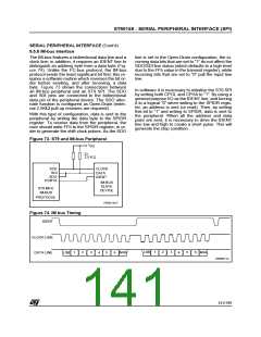
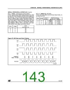
The data on the SDA line is sampled on the low to
high transition of the SCL line.
ferent clock sources and different frequencies can
be interfaced.
2
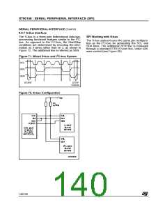
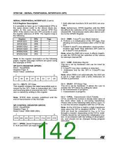
SPI working with an I C-bus
Arbitration Lost
2
To use the SPI with the I C-bus protocol, the SCK
When several masters are sending data on the
SDA line, the following takes place: if the transmit-
ter sends a “1” and the SDA line is forced low by
another device, the ARB flag (SPICR.5) is set and
the SDO buffer is disabled (ARB is reset and the
SDO buffer is enabled when SPIDR is written to
again). When BMS is set, the peripheral clock is
supplied through the INT2 line by the external
clock line (SCL). Due to potential noise spikes
(which must last longer than one INTCLK period to
be detected), RX or TX may gain a clock pulse.
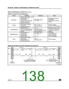
Referring to Figure 70, if device ST9-1 detects a
noise spike and therefore gains a clock pulse, it
will stop its transmission early and hold the clock
line low, causing device ST9-2 to freeze on the 7th
bit. To exit and recover from this condition, the
BMS bit must be reset; this will cause the SPI logic
to be reset, thus aborting the current transmission.
An End of Transmission interrupt is generated fol-
lowing this reset sequence.
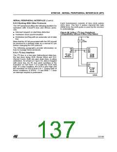
line is used as SCL; the SDI and SDO lines, exter-
nally wire-ORed, are used as SDA. All output pins
must be configured as open drain (see Figure 68).
2
Figure 26 illustrates the typical I C-bus sequence,
comprising 5 phases: Initialization, Start, Trans-
mission, Acknowledge and Stop. It should be not-
ed that only the first 8 bits are handled by the SPI
peripheral; the ACKNOWLEDGE bit must be man-
aged by software, by polling or forcing the SCL
and SDO lines via the corresponding I/O port bits.
2
During the transmission phase, the following I C-
bus features are also supported by hardware.
Clock Synchronization
2
In a multimaster I C-bus system, when several
masters generate their own clock, synchronization
is required. The first master which releases the
SCL line stops internal counting, restarting only
when the SCL line goes high (released by all the
other masters). In this manner, devices using dif-
Figure 70. SPI Arbitration
ST9-1
ST9-2
INTERNAL SERIAL
CLOCK
INTERNAL SERIAL
CLOCK
SCK
SCK
0
0
MSPI
MSPI
CONTROL
CONTROL
LOGIC
LOGIC
1
1
INT 2
INT 2
BHS
BHS
ST9-2-SCK
1
1
2
2
3
3
4
5
5
6
6
7
7
8
SPIKE
4
ST9-1-SCK
VR001410
n
n
139/199
9

 ETC [ ETC ]