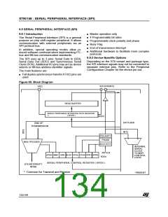
ST90158 - SERIAL PERIPHERAL INTERFACE (SPI)
SERIAL PERIPHERAL INTERFACE (Cont’d)
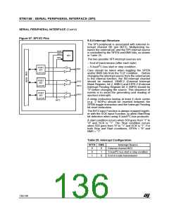
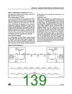
Figure 67. SPI I/O Pins
n
9.5.4 Interrupt Structure
The SPI peripheral is associated with external in-
terrupt channel B0 (pin INT2). Multiplexing be-
tween the external pin and the SPI internal source
is controlled by the SPEN and BMS bits, as shown
in Table 25.
SCK
SDO
SPI
SDI
The two possible SPI interrupt sources are:
– End of transmission (after each byte).
2
– S-bus/I C-bus start or stop condition.
PORT
BIT
SDI
Care should be taken when toggling the SPEN
and/or BMS bits from the “0,0” condition. Before
changing the interrupt source from the external pin
to the internal function, the B0 interrupt channel
should be masked. EIMR.2 (External Interrupt
Mask Register, bit 2, IMBO) and EIPR.2 (External
Interrupt Pending Register bit 2, IMP0) should be
“0” before changing the source. This sequence of
events is to avoid the generating and reading of
spurious interrupts.
LATCH
PORT
BIT
SCK
INT2
LATCH
PORT
BIT
SDO
LATCH
A delay instruction lasting at least 4 clock cycles
(e.g. 2 NOPs) should be inserted between the
SPEN toggle instruction and the Interrupt Pending
bit reset instruction.
INT2
The INT2 input Function is always mapped togeth-
er with the SCK input Function, to allow Start/Stop
2
bit detection when using S-bus/I C-bus protocols.
A start condition occurs when SDI goes from “1” to
“0” and SCK is “1”. The Stop condition occurs
when SDI goes from “0” to “1” and SCK is “1”. For
both Stop and Start conditions, SPEN = “0” and
BMS = “1”.
Table 25. Interrupt Configuration
SPEN BMS
Interrupt Source
External channel INT2
0
0
1
0
1
X
2
S-bus/I C bus start or stop condition
End of a byte transmission
136/199
9

 ETC [ ETC ]