KT0803K
Chip Enable and Mode Control
There is one external pin SW (Pin 8) to enable the chip. The definition is shown below.
Table 5: Pin SW
Input
SW
Chip Mode
IOVDD
Clock Source
0
1
Power off
Power On
N/A
1.6~3.6V
N/A
External crystal or clock
Mute
The FM transmitter can be muted by setting Register MUTE to “1” through I2C programming.
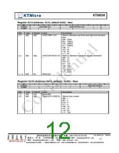
Silence Detection
Bit name
Register location Description
SLNCDIS
Reg 0x12[7]
Setting to 0 to enable the silence detection
silence detection time window
Low threshold voltage of input signal for silence detection
High threshold voltage of input signal for silence detection
# of time when the input signal amplitude is lower than
SLNCTHL
SLNCTIME[2:0]
SLNCTHL[2:0]
SLNCTHH[2:0]
SLNCCNTTHL[2:0]
Reg 0x14[7:5]
Reg 0x12[6:4]
Reg 0x12[3:1]
Reg 0x14[4:2]
SLNCCNTTHH[2:0] Reg 0x16[2:1]
SLNCID Reg 0x0F[2]
# of time when the input signal amplitude is higher than
SLNCTHH
(Read only) Set to 1 when silence is detected.
The silence detection scheme is enabled by setting SLNCDIS to 0.
During the time defined by SLNTIME[2:0], the chip will be muted when the number of time when the
input amplitude is higher than the voltage defined by SLNCTHL[2:0] is lower than SLNCCNTTHL[2:0].
The SLNCID bit is set to 0.
When the input signal amplitude is higher than the voltage defined by SLNCTHH[2:0] and the number of
time when that happens is more than SLNCCNTTHH[2:0], the chip exits from the mute status and the
SLNCID is cleared to 0.
Reset
The global reset is issued after the RSTB pin set to “0” or automatic on-chip power-on reset. After a global
reset, all registers are reset to the default value.
DS-1896P-03 070604
深圳市圣邦达电子有限公司
联系人:邓 生 13798386757 QQ:278815928 E-MAIL:dengwangs@163.com
MSN:dengwangs@hotmail.com 网址:www.sbdsemi.com
传真:068-0755-61351350
13
本资料来源来自互联网,一切版权归属原设计公司,如有与法律相抵触之处,请及时联系我们,我们会及时修改更正

 ETC [ ETC ]