1A Positive Voltage
Regulators (Preliminary)
CYT8117
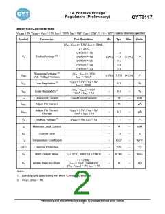
Electrical Characteristic
VIN,MAX ≤ 8V, VIN,MIN – VOUT = 1.5V, IOUT = 10mA, CIN = 10µF, COUT = 22µF, TJ = 0 – 125°C, unless otherwise specified.
Symbol
Parameter
Test Condition
Min
Typ
Max
Units
(VIN - VOUT) = 1.5V, IOUT = 10mA,
TA = 25°C,
CYT8117T15
1.5
1.8
2.5
3.0
3.3
VO
Output Voltage (1)
CYT8117T18
(-2%)
(+2%)
V
CYT8117T25
CYT8117T30
CYT8117T33
Reference Voltage (1)
(Adj. Voltage Version)
(VIN - VOUT) = 1.5V
IOUT = 10mA
VREF
VSR
VLR
(-2%) 1.250 (+2%)
V
V
OUT + 1.5V < VIN < 8V
Line Regulation (1)
Load Regulation (1)
--
--
0.3
0.4
--
--
%
%
IOUT = 10mA
(VIN - VOUT) = 1.5V
10mA ≤ IOUT ≤ 1A
IQ
Quiescent Current
Adjust Pin Current
Fixed Output Version
--
--
10
48
--
--
mA
IADJ
µA
Adjust Pin Current
Change
V
OUT + 1.5V < VIN < 8V
10mA ≤ IOUT ≤ 1A
∆IADJ
--
0.2
--
µA
VD
IO
Dropout Voltage (2)
Minimum Load Current
Current Limit
∆VREF = 1%, IOUT = 1A
--
--
--
--
--
--
1.1
4
--
--
--
--
--
--
V
mA
A
ICL
1.8
TC
Temperature Coefficient
Thermal Protection
RMS Output Noise
0.07
175
0.003
%/°C
°C
OTP
VN
TA = 25°C, 10Hz ≤ f ≤ 10kHz
%VO
f = 120Hz,
RA
Ripple Rejection Ratio
COUT = 22µF (Tantalum),
(VIN - VOUT) = 3V, IOUT = 1A
--
35
--
dB
Notes:
1. Low duty cycle pulse testing with which TJ remains unchanged.
2. ∆VOUT, ∆VREF = 1%.
Preliminary and all contents are subject to change without prior notice.
2

 ETC [ ETC ]