Philips Semiconductors
Product specification
Silicon N-channel dual-gate MOS-FETs
BF998; BF998R
LIMITING VALUES
In accordance with the Absolute Maximum Rating System (IEC 134).
SYMBOL
VDS
PARAMETER
drain-source voltage
drain current
CONDITIONS
MIN.
MAX.
12
UNIT
−
−
−
−
−
−
−
V
ID
30
mA
mA
mA
mW
mW
mW
°C
±IG1
±IG2
Ptot
gate 1 current
10
gate 2 current
10
total power dissipation; BF998
up to Tamb = 60 °C; see Fig.3; note 1
up to Tamb = 50 °C; see Fig.3; note 2
200
200
200
+150
150
Ptot
Tstg
Tj
total power dissipation; BF998R up to Tamb = 50 °C; see Fig.4; note 1
storage temperature
−65
operating junction temperature
−
°C
Notes
1. Device mounted on a ceramic substrate, 8 mm × 10 mm × 0.7 mm.
2. Device mounted on a printed-circuit board.
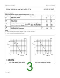
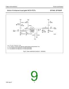
MLA198
MGA002
handbook, halfpage
200
handbook, halfpage
200
(2)
(1)
P
P
tot max
(mW)
tot max
(mW)
100
100
0
0
0
100
200
0
100
200
o
T
(°C)
T
( C)
amb
amb
(1) Ceramic substrate.
(2) Printed-circuit board.
Fig.3 Power derating curves; BF998.
Fig.4 Power derating curve; BF998R.
1996 Aug 01
3

 ETC [ ETC ]