AD7804/AD7805/AD7808/AD7809
APPLICATIONS
AD7808
CLKIN
SDIN
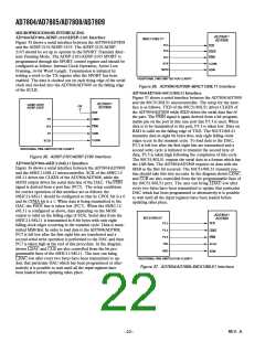
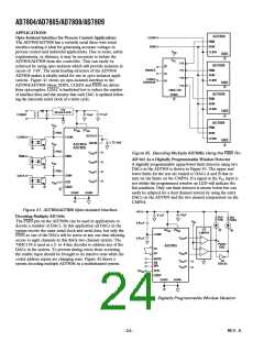
Opto-Isolated Interface for Process Control Applications
The AD7804/AD7808 has a versatile serial three-wire serial
interface making it ideal for generating accurate voltages in
process control and industrial applications. Due to noise, safety
requirements, or distance, it may be necessary to isolate the
AD7804/AD7808 from the controller. This can easily be
achieved by using opto-isolators which will provide isolation in
excess of 3 kV. The serial loading structure of the AD7804/
AD7808 makes it ideally suited for use in opto-isolated appli-
cations. Figure 41 shows an opto-isolated interface to the
AD7804/AD7808 where SDIN, CLKIN and FSIN are driven
from optocouplers. LDAC is hardwired low to reduce the number
of interface lines and this ensures that each DAC is updated follow-
ing the sixteenth serial clock of a write cycle.
FSIN
SDIN
V
V
CLKIN
DD
LDAC
LDAC
LDAC
CC
1Y0
1Y1
1Y2
AD7808
1G
1A
1B
ENABLE
FSIN
SDIN
CODED
ADDRESS
CLKIN
1Y3
74HC139
DGND
AD7808
FSIN
SDIN
CLKIN
+5V
REGULATOR
0.1F
10F
POWER
AD7808
V
V
DD
FSIN
AV
DV
DD
DD
10k⍀
SDIN
CLKIN
REFOUT
CLKIN
FSIN
CLKIN
FSIN
LDAC
1 TO 10nF
REFIN
AD7804/
AD7808
DD
10k⍀
V
V
A
B
OUT
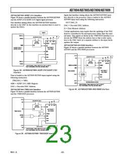
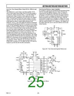
Figure 42. Decoding Multiple AD7808s Using the FSIN Pin
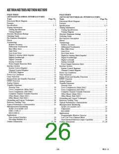
AD7805 As a Digitally Programmable Window Detector
A digitally programmable upper/lower limit detector using two
DACs in the AD7805 is shown in Figure 43. The upper and
lower limits for the test are loaded to DACs A and B that in
turn set the limits on the CMP04. If a signal at the VIN input is
not within the programmed window an LED will indicate the
fail condition. Only one limit detector is shown below but can
easily be adapted for a dual channel system by using the extra
DACs on the AD7805 and the two unused comparators on the
CMP04.
OUT
V
DD
10k⍀
V
V
C
D
OUT
OUT
SDIN
DATA
CLR
V
1
DD
LDAC
DGND
AGND
Figure 41. AD7804/AD7808 Opto-Isolated Interface
+5V
10F
0.1F
Decoding Multiple AD7808s
1k⍀
1k⍀
PASS
FAIL
The FSIN pin on the AD7808s can be used in applications to
decode a number of DACs. In this application all DACs in the
system receive the same serial clock and serial data, but only the
FSIN to one of the DACs will be active at any one time allowing
access to eight channels in this thirty-two channel system. The
74HC139 is used as a 2- to 4-line decoder to address any of the
DACs in the system. To prevent timing errors from occurring
the enable input should be brought to its inactive state while the
coded address inputs are changing state. Figure 42 shows a
system decoding multiple AD7808s in a multichannel system.
V
IN
0.01F
0.01F
1/2
CMP04
AV
DV
DD
DD
COMP
V
A
B
OUT
OUT
PASS/
FAIL
AD7805
D9
D0
V
MODE
1/6
74HC05
V
V
C
D
OUT
CS
WR
OUT
DV
DD
CLR
LDAC
DGND
AGND
Figure 43. Digitally Programmable Window Detector
–24–
REV. A

 ETC [ ETC ]