AD7804/AD7805/AD7808/AD7809
Again fast interface timing allows the AD7805/AD7809 inter-
face directly to the processor. Data is loaded to the AD7805/
AD7809 input latch using the following instruction:
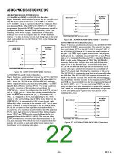
AD7805/AD7809–ADSP-2101 Interface
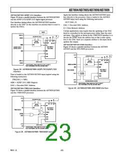
Figure 38 shows a parallel interface between the AD7805/AD7809
and the ADSP-2101/ADSP-2103 digital signal processor.
OUT DAC, D.
Fast interface timing allows the AD7805/AD7809 interface
directly to the DSP. In this interface an external timer is used to
update the DACs.
DAC = Decoded DAC Address.
D = Data Memory Address.
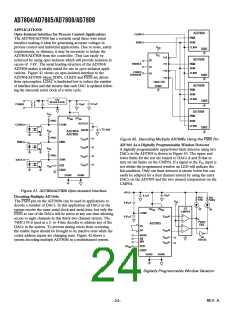
Certain applications may require that the updating of the DAC
latch be controlled by the microprocessor rather than the exter-
nal timer. One option as shown in the TMS32020 interface is to
decode the LDAC from the address bus so that a write opera-
tion to the DAC latch (at a separate address to the input latch)
updates the output.
TIMER
DMA14
ADDRESS BUS
DMA0
A2**
A0 A1
ADDR
DECODE
LDAC
MODE
DMS
EN
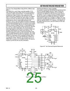
AD7805/AD7809–8051/8088 Interface
CS
Figure 40 shows a parallel interface between the AD7805/
AD7809 and the 8051/8088 processors.
AD7805*/
AD7809
ADSP-2101*/
ADSP-2103*
WR
WR
DB9
DB0
A15
ADDRESS BUS
A8
A0 A1 A2**
ADDR
DMD15
DMD0
DATA BUS
CS
DECODE
MODE
PSEN OR DEN
EN
LDAC
**ADDITIONAL PINS OMITTED FOR CLARITY
**A2 CONTAINED ON THE AD7809 ONLY
WR
WR
Figure 38. AD7805/AD7809–ADSP-2101/ADSP-2103
Interface
AD7805*/
AD7809
8051/8088
ALE
OCTAL
LATCH
DB9
DB0
Data is loaded to the AD7805/AD7809 input register using the
following instruction:
DM(DAC) = MR0,
AD7
AD0
ADDRESS/DATA BUS
MR0 = ADSP-2101 MR0 Register.
DAC = Decoded DAC Address.
**ADDITIONAL PINS OMITTED FOR CLARITY
**A2 CONTAINED ON THE AD7809 ONLY
Figure 40. AD7805/AD7809–8051/8088 Interface
AD7805/AD7809–TMS32020 Interface
Figure 39 shows a parallel interface between the AD7805/AD7809
and the TMS32020 processor.
A15
ADDRESS BUS
A0
A0 A1 A2**
ADDR
CS
DECODE
EN
IS
AD7805*/
AD7809
TMS32020
LDAC
STRB
WR
R/W
DB9
DB0
D15
D0
DATA BUS
**ADDITIONAL PINS OMITTED FOR CLARITY
**A2 CONTAINED ON THE AD7809 ONLY
Figure 39. AD7805/AD7809–TMS32020 Interface
REV. A
–23–

 ETC [ ETC ]