AD7804/AD7805/AD7808/AD7809
MICROPROCESSOR INTERFACING
AD7804*/
AD7808
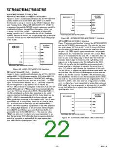
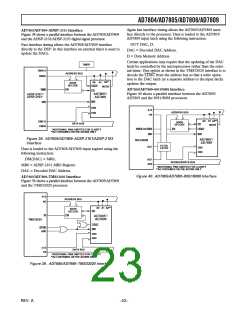
AD7804/AD7808–ADSP-2101/ADSP-2103 Interface
Figure 35 shows a serial interface between the AD7804/AD7808
and the ADSP-2101/ADSP-2103. The ADSP-2101/ADSP-
2103 should be set up to operate in the SPORT Transmit Alter-
nate Framing Mode. The ADSP-2101/ADSP-2103 SPORT is
programmed through the SPORT control register and should be
configured as follows: Internal Clock Operation, Active Low
Framing, 16-bit Word Length. Transmission is initiated by
writing a word to the TX register after the SPORT has been
enabled. The data is clocked out on each rising edge of the serial
clock and clocked into the AD7804/AD7808 on the falling edge
of the SCLK.
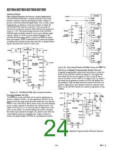
68HC11/68L11*
PC5
CLR
PC6
LDAC
FSIN
PC7
SCK
CLKIN
SDIN
MOSI
*ADDITIONAL PINS OMITTED FOR CLARITY
Figure 36. AD7804/AD7808–68HC11/68L11 Interface
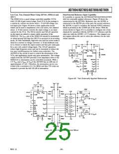
AD7804/AD7808–80C51/80L51 Interface
Figure 37 shows a serial interface between the AD7804/AD7808
and the 80C51/80L51 microcontroller. The setup for the inter-
face is as follows, TXD of the 80C51/80L51 drives CLKIN of
the AD7804/AD7808 while RXD drives the serial data line of
the part. The FSIN signal is again derived from a bit program-
mable pin on the port in this case port line P3.3 is used. When
data is to be transmitted to the part, P3.3 is taken low. Data on
RXD is valid on the falling edge of TXD. The 80C51/80L51
transmits data in eight bit bytes thus only eight falling clock
edges occur in the transmit cycle. To load data to the DAC,
P3.3 is left low after the first eight bits are transmitted and a
second write cycle is initiated to transmit the second byte of
data, P3.3 is taken high following the completion of this cycle.
The 80C51/80L51 outputs the serial data in a format which has
the LSB first. The AD7804/AD7808 requires its data with the
MSB as the first bit received. The 80C51/80L51 transmit rou-
tine should take this into account. In the diagram shown LDAC
and CLR are also controlled from the bit programmable lines of
the 80C51/80L51 port. The user can bring LDAC low after
every two bytes have been transmitted to update that particular
DAC which has been programmed or alternatively it is possible
to wait until all the input registers have been loaded before
updating takes place.
AD7804*/
AD7808
ADSP-2101/
ADSP-2103*
+5V
CLR
FO
TFS
DT
LDAC
FSIN
SDIN
CLKIN
SCLK
*ADDITIONAL PINS OMITTED FOR CLARITY
Figure 35. ADSP-2101/ADSP-2103 Interface
AD7804/AD7808–68HC11/68L11 Interface
Figure 36 shows a serial interface between the AD7804/AD7808
and the 68HC11/68L11 microcontroller. SCK of the 68HC11/
68L11 drives the CLKIN of the AD7804/AD7808, while the
MOSI output drives the serial data line of the DAC. The FSIN
signal is derived from a port line (PC7). The setup conditions
for correct operation of this interface are as follows: the
68HC11/68L11 should be configured so that its CPOL bit is a 0
and its CPHA bit is a 1. When data is being transmitted to the
DAC the FSIN line is taken low (PC7). When the 68HC11/
68L11 is configured as above, data appearing on the MOSI
output is valid on the falling edge of SCK. Serial data from the
68HC11/68L11 is transmitted in 8-bit bytes with only eight
falling clock edges occurring in the transmit cycle. Data is trans-
mitted MSB first. In order to load data to the AD7804/AD7808,
PC7 is left low after the first eight bits are transferred and a
second serial write operation is performed to the DAC and then
PC7 is taken high at the end of this procedure. In the diagram
shown LDAC and CLR are also controlled from the bit pro-
grammable lines of the 68HC11/68L11. The user can bring
LDAC low after every two bytes have been transmitted to up-
date that particular DAC which has been programmed or alter-
natively it is possible to wait until all the input registers have
been loaded before updating takes place.
AD7804*/
80C51/80L51*
AD7808
CLR
P3.5
P3.4
P3.3
TXD
LDAC
FSIN
SCLK
SDIN
RXD
*ADDITIONAL PINS OMITTED FOR CLARITY
Figure 37. AD7804/AD7808–80C51/80L51 Interface
–22–
REV. A

 ETC [ ETC ]