AD7804/AD7805/AD7808/AD7809
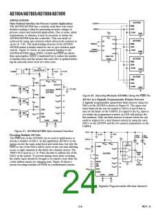
MAIN DAC RANGE
32
2
62
V
32
V
32
V
32
BIAS
BIAS
BIAS
1
31
63
3
33
61
V
V
V
V
V
BIAS
V
32
BIAS
BIAS
BIAS
32
32
32
32 BIAS
32
BIAS
SUB DAC
RANGE
CHANNEL RANGE MIN CODE LOADED TO SUB DAC
CHANNEL RANGE CENTER CODE LOADED TO SUB DAC
CHANNEL RANGE MAX CODE LOADED TO SUB DAC
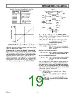
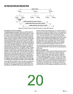
Figure 28. Pictorial View of Transfer Function for Any DAC Channel
Grounding and Layout Techniques
should be shielded with analog ground. To reduce the noise on
this reference it should be decoupled with a 0.01 µF capacitor to
analog ground, keeping the capacitor as close as possible to the
device. The comp pin which is the output from the internal
VDD/2 reference is located next to VOUTD on the DAC and is
sensitive to noise pickup and feedthrough from the DAC output
and thus should be shielded with analog ground to keep this
reference point as quiet as possible. The comp pin should be
decoupled both to AVDD and AGND with 1–10 nF ceramic
capacitors. The external REFIN pin should also be shielded
with analog ground from the digital pins located next to it.
To obtain optimum performance from the AD7804/AD7805/
AD7808/AD7809 care should be taken with the layout. Causes
for concern would be feedthrough from the interface bus onto
the analog circuitry particularly the reference pins and ground
loops. The board should be designed such that the analog and
digital sections are separated as much as possible. Ground plan-
ing and shielding should be used as much as possible. Digital
and analog ground planes should only be joined in one place to
avoid ground loops. The ideal place to join the ground planes is
at the analog and digital ground pins of the DAC. Alternatively
a star ground should be established on the board to which all
other grounds are returned. Good decoupling is important in
achieving optimum performance. All supplies, analog or digital,
should be decoupled with 10 µF tantalum and 0.1 µF ceramic
capacitors to their respective grounds, and should be as close as
possible to the pins of the device. The main aim of the bypass-
ing element is to maximize the charge stored in the bypass loop
while simultaneously minimizing the inductance of this loop.
Inductance in the loop acts as an impedance to high frequency
transients and results in power supply spiking. By keeping the
decoupling as close as possible to the device, the loop area is kept
to a minimum thus reducing the possibility of power supply spikes.
The same precautions should be taken with the reference pins
on the AD7804/AD7808 to reduce the risk of noise pickup and
feedthrough.
Reference Settling Time
With the REFOUT on the AD7804/AD7805/AD7808/AD7809
decoupled with a 0.01 µF capacitor to AGND it takes the
REFOUT approximately 2 ms to fully settle after taking the
device out of power down. When this capacitor is reduced to
1 nF the settling time reduces to 150 µs. The size of the capaci-
tor required on the REFOUT depends to a large extent on the
layout, if the REFOUT is well shielded with AGND the size of
the capacitor can be reduced thus reducing the settling time for
the reference. The internal VDD/2 reference provided at the
comp pin when decoupled with a 1 nF capacitor to both AVDD
and AGND has very fast settling time, typically less than 500 ns.
On the AD7805 the REFOUT pin of the device is located next
to the DB9 of the data bus, to reduce the risk of digital feed-
through and noise being coupled from the digital section onto
the reference, the REFOUT pin and any trace connected to it
–20–
REV. A

 ETC [ ETC ]