AD7804/AD7805/AD7808/AD7809
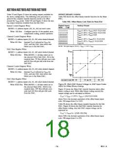
Configuring the AD7805/AD7809 for Twos Complement Coding
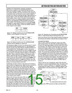
Figure 24 shows a typical configuration for the AD7805/AD7809.
The circuit can be used for either 3.3 V or 5 V operation and uses
the internal VDD/2 as the reference for the part and 10-bit paral-
lel interfacing is used. The following are the steps required to
operate the Main DACs in this part.
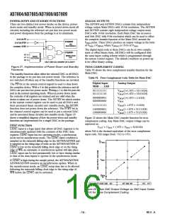
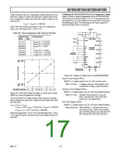
Table VII shows the twos complement transfer function for the
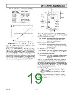
Sub DAC. Figure 23 shows the Sub DAC transfer function for
twos complement coding. Any Sub DAC output voltage can be
expressed as:
V
OUT" = VBIAS/16 × (NB/256)
where NB is the decimal equivalent of the twos complement
input code. NB ranges from –128 to +127.
+3.3V/+5V
Table VII. Twos Complement Code Table for Sub DAC
0.1F
0.1F
10F
Digital Input
MSB . . . LSB
Analog Input
0.01F
0.01F
AV
DV
DD
DD
COMP
REFIN
01111111
01111111
00000001
00000000
11111111
10000001
10000000
(VBIAS/16) × (127/256)
(VBIAS/16) × (126/256)
(VBIAS/16) × (1/256)
0
(–VBIAS/16) × (1/256)
(–VBIAS/16) × (127/256)
(–VBIAS/16) × (128/256)
REFOUT
A2*
A0
AD7805/
AD7809
V
A
B
OUT
A1
D9
D0
DIGITAL
INTERFACE
V
OUT
MODE
CS
V
C
D
OUT
V
127
256
BIAS
16
WR
V
DV
DD
CLR
OUT
LDAC
AGND
DGND
*USED ON THE
AD7809 ONLY
0
Figure 24. Typical Configuration for AD7805/AD7809
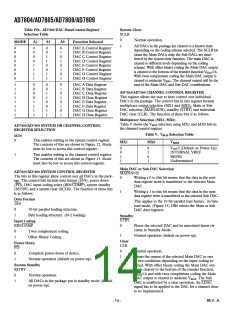
System Control Register Write:
MODE = 0, address inputs (A2, A1, A0) are don’t cares.
V
128
256
BIAS
16
Write 020 Hex Configure part for 10-bit parallel, twos
complement coding, normal operation
Channel Control Register Write:
80
81
FF
01
7F
DAC INPUT CODE
00
7E
MODE = 0, address inputs (A2, A1, A0) select desired channel.
Figure 23. Sub DAC Output Voltage vs. DAC Input Codes
(HEX) for Twos Complement Coding
Write 011 Hex
Internal VDD/2 selected as VBIAS for
DAC, and any DAC data writes that
follow are to the Main DAC.
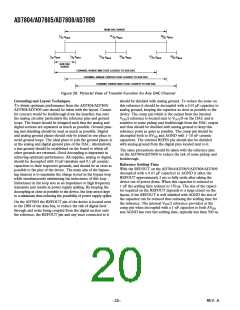
The total output for a single channel when using twos comple-
ment coding is the sum of the voltage from the Main DAC and
the Sub DAC.
DAC Data Register Write:
MODE = 1, address inputs (A2, A1, A0) select desired channel.
VOUT = VOUT' + VOUT
"
= VBIAS + 1.875 × VBIAS × (NA/1024) + VBIAS/16 × (NB/256)
Write XXX Hex With MODE = 1 all data writes are to
the selected DAC. XXX is the required
= VBIAS × (1 + 1.875 × NA/1024 + NB/4096)
data. 200 Hex will give zero scale and 1FF
Hex will give full scale from the DAC.
where NA ranges from –512 to +511 and NB ranges from –128 to
+127. Figure 28 shows a pictorial view of the transfer function for
any DAC.
REV. A
–17–

 ETC [ ETC ]