AD7804/AD7805/AD7808/AD7809
POWER-DOWN AND STANDBY FUNCTIONS
ANALOG OUTPUTS
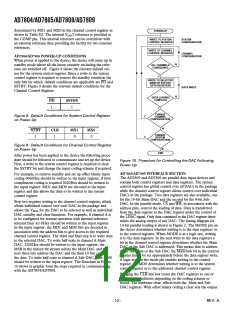
There are two distinct low power modes on the device, power-
down mode and standby mode. When in power-down mode all
circuitry including the reference are put into low power mode
and power dissipation from the package is at its minimum.
The AD7804 and AD7805 DACs contain four independent
voltage output Main DACs with 10-bit resolution. The AD7808
and AD7809 contain eight independent voltage output main
DACs with 10-bit resolution. Each Main DAC has an associ-
ated Sub DAC with 8-bit resolution which can be used to offset
the complete transfer function of the Main DAC around the
VBIAS point. These DACs produce an output voltage in the form
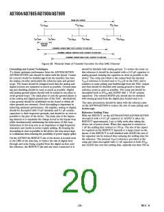
SYSTEM PD
STANDBY
SYSTEM STBY
INT
REFERENCE
of VBIAS ±VSWING where VSWING is 15/16 of VBIAS
.
CHANNEL STBY
The digital input code to these DACs can be in twos comple-
ment or offset binary form. All DACs will be configured with
the same input coding scheme which is programmed through
the system control register. The default condition on power-up
is for offset binary coding.
STANDBY
A2
MAIN & SUB
ADDR
A1
A0
DAC
DECODER
ONLY ONE DAC SHOWN FOR CLARITY
Figure 21. Implementation of Power-Down and Standby
Functions
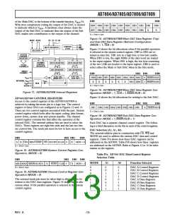
TWOS COMPLEMENT CODING
Table VI shows the twos complement transfer function for the
Main DAC.
The standby functions allow either the selected DAC or all DACs
in the package to be put into low power mode. The reference is
not switched off when any of the standby functions are invoked.
Table VI. Twos Complement Code Table for Main DAC
Digital Input
MSB . . . LSB
Analog Output
The PD bit in the system control register is used to shut down
the complete device. With a 0 in this position the reference and all
DACs are put into low power mode. Writing a 1 to this bit puts the
part in the normal operating mode. When in power-down mode
the contents of all registers are retained and are valid when the
device is taken out of power down. The SSTBY bit which resides
in the system control register can be used to put all DACs and
their associated linear circuitry into standby mode, the SSTBY
function does not power down the reference. The STBY bit in
the channel control register can be used to put a selected DAC
and its associated linear circuitry into standby mode. Figure 18
shows a simplified diagram of how the power-down and standby
functions are implemented for a single DAC in the package.
0111111111
0111111110
V
BIAS(1+1.875 × 511/1024)
VBIAS(1+1.875 × 510/1024)
0000000001
0000000000
VBIAS(1+1.875 × 1/1024)
VBIAS
1111111111
VBIAS(1–1.875 × 1/1024)
1000000001
1000000000
V
BIAS(1–1.875 × 511/1024)
VBIAS(1–1.875 × 512/1024)
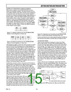
Figure 22 shows the Main DAC transfer function for twos
complement coding. Any Main DAC output voltage can be
expressed as:
LDAC FUNCTION
V
OUT' = VBIAS + 1.875 × VBIAS × NA/1024
LDAC input is a logic input that allows all DAC registers to be
simultaneously updated with the contents of the DAC data
registers. LDAC input has two operating modes, a synchronous
mode and an asynchronous mode. The LDAC input condition is
sampled on the sixteenth falling edge on the AD7804/AD7808 and
is sampled on the rising edge of write on the AD7805/AD7809. If
LDAC is low on the sixteenth falling clock edge or on the rising
edge of WR, an automatic or synchronous update will take place.
LDAC input can be tied permanently low or have timing similar
to that of the data inputs to operate in the synchronous mode.
where NA is the decimal equivalent of the twos complement
input code. NA ranges from –512 to +511.
31
V
BIAS
16
V
BIAS
If LDAC is high during the sample period, the AD7804/AD7805/
AD7808/AD7809 assumes an asynchronous update. When in
the asynchronous mode, an LDAC setup time has to be allowed
following the sixteenth falling clock edge or the rising edge of
WR before the LDAC can be activated.
V
BIAS
16
200 201
3FF
001
000
1FE 1FF
DAC INPUT CODE
Figure 22. Main DAC Output Voltage vs. DAC Input Codes
(HEX) for Twos Complement Coding
–16–
REV. A

 ETC [ ETC ]