AD7804/AD7805/AD7808/AD7809
POWER-UP CONDITIONS (POWER-ON RESET)
When power is applied to the AD7805/AD7809 the device
powers up in a known condition. The device powers up in sys-
tem standby (SSTBY) mode where all DACs in the package are
in low power mode, the reference is active and the outputs of
the DACs are connected internally through a high impedance to
ground. Figure 17 show the default conditions for the system
control register. Since a write to the system control register is
required to remove the standby condition, relevant default con-
ditions are only applicable for PD and SSTBY in the system
control register. The following are the bits in the channel con-
trol register for which default conditions are applicable, STBY,
CLR, MX1 and MX0. Figure 18 shows the default conditions
for the channel control register.
START
WRITE TO SYSTEM
CONTROL REGISTER
Y
WRITE TO
MAIN DAC
WRITE TO CHANNEL
CONTROL REGISTER
N
Y
WRITE TO
SUB DAC
WRITE TO MAIN DAC
DATA REGISTER
WRITE TO CHANNEL
CONTROL REGISTER
N
WRITING
COMPLETE
Y
WRITE TO SUB DAC
DATA REGISTER
RECONFIGURE
SYSTEM
Y
N
PD
SSTBY
N
WRITING
COMPLETE
END
1
1
Y
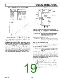
Figure 17. Default Conditions for the AD7805/AD7809
System Control Register on Power-Up
Figure 19. Flowchart for Controlling the AD7805/AD7809
DACs in 10-Bit Parallel Mode Following Power-Up
STBY
CLR
MX1
MX0
mode as the selection can be made using the hardware bit DB0 and
this will reduce the software overheads when accessing the DACs.
1
1
0
0
CLEAR FUNCTIONS
Figure 18. Default Conditions for the AD7805/AD7809
Channel Control Register on Power-Up
There are three methods of clearing the output of the Main
DAC in these devices. The first is the external hardware clear.
An active low logic signal applied to this pin clears all the DACs
in the package. The voltage to which the output is cleared will
depend on the input coding selected. The Main DAC outputs
are cleared to midscale (VBIAS) in twos complement format and
to the bottom of the transfer function (VBIAS/16) in offset binary
format. The second way of clearing the main DACs is a software
clear by asserting the SCLR bit in the system control register of
the part. Writing a one to this bit clears all DACs in the pack-
age. The third method of clearing a DAC is to write a one to the
CLR bit in the channel control register. This differs from that of
the system control register in that only the selected DACs out-
put is cleared. The channel clear requires an LDAC pulse to
activate it.
The flowchart in Figure 19 shows the steps necessary to control
the AD7805/AD7809 following power-on. This flowchart de-
tails the necessary steps when using the AD7805/AD7809 in its
10-bit parallel mode. The first step is to write to the system
control register to clear the SSTBY bit and to configure the part
for 10-bit parallel mode and select the required coding scheme.
The next step is to determine whether writing is to the Main or
Sub DAC. This is achieved by writing to the channel control
register. Other bits that need to be configured in the channel
control register are MX1 and MX0 which determine the source
of the VBIAS for the selected DAC and the channel STBY and
channel CLR bits need to be configured as desired. Once writ-
ing to the channel control register is complete, data can now be
written to the selected Main or Sub DAC.
There is only one way of clearing the output of the Sub DAC
and that is to use the external hardware clear. The output of the
Sub DAC is cleared to midscale (0 V) regardless of the input
coding being used. Figure 20 shows a simplified diagram of the
implementation of the clear functions for a single DAC in the
package.
Parallel data can also be written to the device in 8+2 format to
allow interface to 8-bit processors. Eight-bit mode is invoked by
writing a one to the 10/8 bit in the system control register.
When in the 8-bit mode the two unused data bits (DB1 and
DB0) are used as hardware control bits and have the same tim-
ing characteristics as the address inputs. DB1 is a don’t care bit
when writing to both the system and channel control registers;
DB0 acts as the mode select bit and must be low to enable writ-
ing to the system control register and when high enables access
to the channel control register.
EXT CLR
SYSTEM CLR
CLR
SUB DAC
CHANNEL CLR
LDAC
CLR
When in the 8-bit data write mode, DB1 acts as a low byte and
high byte enable, when low data is written to the 8 MSBs of the
DAC and when high data is written to the two LSBs. DB0 acts
as a bit to select writing to the Main or Sub DAC. When DB0 is
low, writing is to the Main DAC, and when high, writing is to
the Sub DAC data register. In the 8+2 mode the channel con-
trol register does not have to be accessed to switch between
writing to the Main and Sub DACs as in the 10-bit parallel
A2
MAIN DAC
ADDR
A1
DECODER
A0
ALL OTHER CIRCUITRY OMITTED FOR CLARITY
Figure 20. CLR Functions for Main and Sub DACs
REV. A
–15–

 ETC [ ETC ]