Datasheet
TD1410
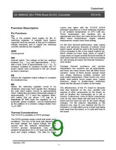
2A 380KHZ 20V PWM Buck DC/DC Converter
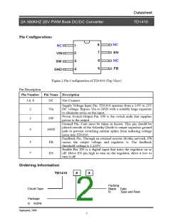
Pin Configurations
Figure 2 Pin Configuration of TD1410 (Top View)
Pin Description
Pin Number Pin Name Description
1,6, 8
NC
Not Connect.
Supply Voltage Input Pin. TD1410 operates from a 3.6V to 23V
DC voltage. Bypass Vin to GND with a suitably large capacitor
to eliminate noise on the input.
2
Vin
Power Switch Output Pin. SW is the switch node that supplies
power to the output.
Ground Pin. Care must be taken in layout. This pin should be
placed outside of the Schottky Diode to output capacitor ground
path to prevent switching current spikes from inducing voltage
noise into TD1410.
3
4
SW
GND
Feedback Pin. Through an external resistor divider network, FB
senses the output voltage and regulates it. The feedback
threshold voltage is 1.235V.
Enable Pin. EN is a digital input that turns the regulator on or
off .Drive EN pin high to turn on the regulator, drive it low to
turn it off.
5
7
FB
EN
Ordering Information
X
TD1410
X
Packing
Blank: Tube
Circuit Type
R:
Type and Reel
Package
S: SOP8
September, 2006
2

 ETC [ ETC ]