RTC6701
DEC 2005
Preliminary
Data Sheet
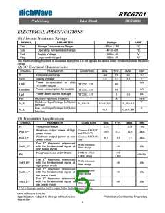
ELECTRICAL SPECIFICATIONS
(1) Absolute Maximum Ratings
SYMBOL
PARAMETER
Ratings
UNIT
Storage Temperature Range
Operating Temperature Range
Supply Voltage
-65 to +150
-40 to +85
-0.5 to +5
-0.5 to +5
Tstr
Totr
Vdd
Vlog
°C
°C
V
Logic control signal
V
The maximum rating must not be exceeded at any time. Do not operate the device under conditions outside the above
ratings.
(2)DC Electrical Characteristics
SYMBOL
PARAMETER
Temperature Range
Supply Voltage
CONDITION
MIN.
-40
TYP.
25
MAX.
85
UNIT
Tj
-
°C
V
VDD
I_RF
3.1
3.3
3.5
mA
Power consumption for chip
(+12dBm output)
TT 25C, 3.3V
49
54
mA
uA
Power consumption for module
I_module
TT 25C, 3.3V
TT 25C, 3.3V
Power down current leakage
I_pd
Fref
1
8
10
Oscillator operating frequency
MHz
V
High Level Input Voltage for Digital
Interface
V_IH
V_IL
V_IO=3V
0.7xV_IO
-0.3
V_IO+0.3
0.3xV_IO
Low Level Input Voltage for Digital
Interface
V
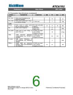
(3) Transmitter Specifications
SYMBOL
PARAMETER
CONDITION
MIN.
TYP.
MAX.
UNIT
Fc
2.37
2.51
GHz
Frequency Range
Connect PAOUT1
and PAOUT2
Maximum output power at high
power mode
Pout_H*
Pout_L*
10.5
0.5
11.5
1.5
12.5
2.5
dBm
dBm
Connect PAOUT1
only
Maximum output power at low
power mode
The 2nd Harmonic referenced
with the fundamental signal at
high power mode
With reference
filter design
2ndH_H*
PN
-30
dBc
dBc/Hz
dBc
100KHz offset
1MHz offset
-85
The phase noise at 2414GHz
-110
The 3rd Harmonic referenced
with the fundamental signal at
high power mode
The 2nd Harmonic referenced
with the fundamental signal at
low power mode
The 3rd Harmonic referenced
with the fundamental signal at
low power mode
With reference
filter design
3rdH_H*
-40
-30
-40
With reference
filter design
2ndH_L*
3rdH_L*
dBc
dBc
With reference
filter design
* All with proper match at the PA output, before further ceramic filtering.
www.richwave.com.tw
Specifications subject to change without notice
Rev V.004
Preliminary Confidential Proprietary
5

 ETC [ ETC ]