Data Sheet
June 1999
ORCA Series 2 FPGAs
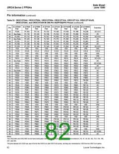
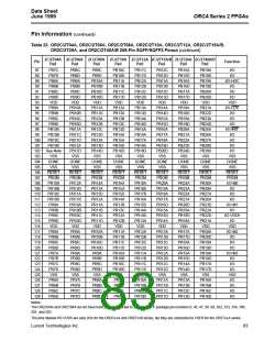
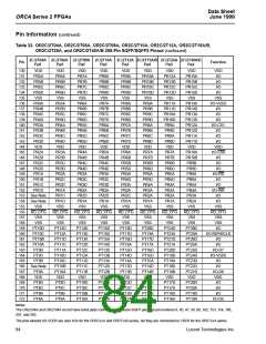
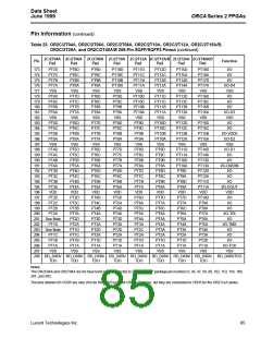
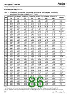
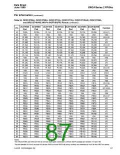
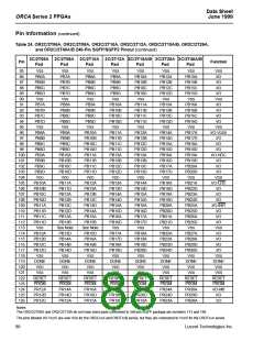
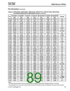
Pin Information (continued)
Table 24. OR2C/2T06A, OR2C/2T08A, OR2C/2T10A, OR2C/2T12A, OR2C/2T15A/B, OR2C/2T26A,
and OR2C/2T40A/B 240-Pin SQFP/SQFP2 Pinout
2C/2T06A 2C/2T08A 2C/2T10A 2C/2T12A 2C/2T15A/B 2C/2T26A 2C/2T40A/B
Pin
Function
Pad
Pad
Pad
Pad
Pad
Pad
Pad
1
VSS
VSS
VDD
VSS
VDD
VSS
VDD
VSS
VDD
VSS
VDD
VSS
VSS
VDD
I/O
2
VDD
VDD
3
PL1D
PL1C
PL1B
PL1A
VSS
PL1D
PL1B
PL1A
PL2D
VSS
PL1D
PL1B
PL1A
PL2D
VSS
PL1D
PL1C
PL1B
PL2D
VSS
PL1D
PL1C
PL1B
PL2D
VSS
PL1D
PL1C
PL1B
PL2D
VSS
PL1D
PL1A
4
I/O
5
PL2D
PL3D
VSS
I/O
6
I/O-A0
VSS
I/O-VDD5
I/O
7
8
PL2D
PL2C
PL2B
PL2A
PL3D
PL3C
PL3B
PL3A
VDD
PL3D
PL3C
PL3B
PL3A
PL4D
PL4C
PL4B
PL4A
VDD
PL3D
PL3C
PL3B
PL3A
PL4A
PL5C
PL5B
PL5A
VDD
PL3D
PL3A
PL4D
PL4A
PL5A
PL6D
PL6B
PL6A
VDD
PL4D
PL4A
PL5D
PL5A
PL6A
PL7D
PL7B
PL7A
VDD
PL4D
PL4A
PL5D
PL5A
PL6A
PL7D
PL7B
PL7A
VDD
PL5D
PL6D
PL7D
PL8D
PL9A
9
10
11
12
13
14
15
16
17
18
19
20
21
22
23
24
25
26
27
28
29
30
31
32
33
34
35
36
37
38
39
40
41
42
I/O
I/O-A1
I/O-A2
I/O
PL10D
PL10B
PL10A
VDD
I/O
I/O-A3
VDD
I/O
PL4D
PL4C
PL4B
PL4A
PL5D
PL5C
PL5B
PL5A
VSS
PL5D
PL5C
PL5B
PL5A
PL6D
PL6C
PL6B
PL6A
VSS
PL6D
PL6C
PL6B
PL6A
PL7D
PL7C
PL7B
PL7A
VSS
PL7D
PL7C
PL7B
PL7A
PL8D
PL8C
PL8B
PL8A
VSS
PL8D
PL8C
PL8B
PL8A
PL9D
PL9C
PL9B
PL9A
VSS
PL8D
PL8A
PL9D
PL9A
PL10D
PL10A
PL11D
PL11A
VSS
PL11D
PL11A
PL12D
PL12A
PL13D
PL13A
PL14D
PL14A
VSS
I/O
I/O
I/O-A4
I/O-A5
I/O
I/O
I/O-A6
VSS
I/O
PL6D
PL6C
PL6B
PL6A
VDD
PL7D
PL7C
PL7B
PL7A
VDD
PL8D
PL8C
PL8B
PL8A
VDD
PL9D
PL9C
PL9B
PL9A
VDD
PL10D
PL10C
PL10B
PL10A
VDD
PL12D
PL12C
PL12B
PL12A
VDD
PL15D
PL15C
PL15B
PL15A
VDD
I/O
I/O
I/O-A7
VDD
I/O
PL7D
PL7C
PL7B
PL7A
VSS
PL8D
PL8C
PL8B
PL8A
VSS
PL9D
PL9C
PL9B
PL9A
VSS
PL10D
PL10C
PL10B
PL10A
VSS
PL11D
PL11C
PL11B
PL11A
VSS
PL13D
PL13C
PL13B
PL13A
VSS
PL16D
PL16C
PL16B
PL16A
VSS
I/O-VDD5
I/O
I/O-A8
VSS
I/O-A9
I/O
PL8D
PL8C
PL8B
PL8A
PL9D
PL9C
PL9B
PL9D
PL9C
PL9B
PL9A
PL10D
PL10C
PL10B
PL10D
PL10C
PL10B
PL10A
PL11D
PL11C
PL11B
PL11D
PL11C
PL11B
PL11A
PL12D
PL12C
PL12B
PL12D
PL12C
PL12B
PL12A
PL13D
PL13C
PL13B
PL14D
PL14A
PL15D
PL15A
PL16D
PL16A
PL17D
PL17D
PL17A
PL18D
PL18A
PL19D
PL19A
PL20D
I/O
I/O-A10
I/O
I/O
I/O
Notes:
The OR2C/2T08A and OR2C/2T10A do not have bond pads connected to 240-pin SQFP package pin numbers 113 and 188.
The pins labeled I/O-VDD5 are user I/Os for the OR2CxxA and OR2TxxB series, but they are connected to VDD5 for the OR2TxxA series.
86
Lucent Technologies Inc.

 ETC [ ETC ]