Data Sheet
June 1999
ORCA Series 2 FPGAs
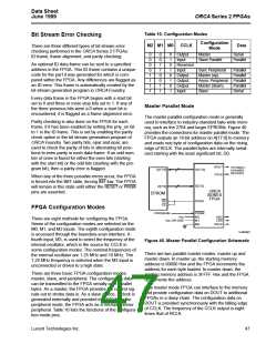
Table 10. Configuration Modes
Bit Stream Error Checking
Configuration
Mode
M2 M1 M0
CCLK
Output
Input
Reserved
Input
Output
Output
Output
Input
Data
Serial
There are three different types of bit stream error
checking performed in the ORCA Series 2 FPGAs:
ID frame, frame alignment, and parity checking.
0
0
0
0
1
1
1
1
0
0
1
1
0
0
1
1
0
1
0
1
0
1
0
1
Master
Slave Parallel
Parallel
An optional ID data frame can be sent to a specified
address in the FPGA. This ID frame contains a unique
code for the part it was generated for which is com-
pared within the FPGA. Any differences are flagged as
an ID error. This frame is automatically created by the
bit stream generation program in ORCA Foundry.
Sync Peripheral
Master (up)
Async Peripheral Parallel
Master (down)
Slave
Parallel
Parallel
Parallel
Serial
Every data frame in the FPGA begins with a start bit
set to 0 and three or more stop bits set to 1. If any of
the three previous bits were a 0 when a start bit is
encountered, it is flagged as a frame alignment error.
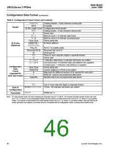
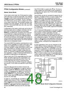
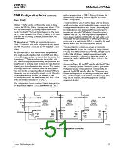
Master Parallel Mode
The master parallel configuration mode is generally
used to interface to industry-standard byte-wide mem-
ory, such as the 2764 and larger EPROMs. Figure 40
provides the connections for master parallel mode. The
FPGA outputs an 18-bit address on A[17:0] to memory
and reads one byte of configuration data on the rising
edge of RCLK. The parallel bytes are internally serial-
ized starting with the least significant bit, D0.
Parity checking is also done on the FPGA for each
frame, if it has been enabled by setting the prty_en bit
to 1 in the ID frame. This is set by enabling the parity
check option in the bit stream generation program of
ORCA Foundry. Two parity bits, opar and epar, are
used to check the parity of bits in alternating bit posi-
tions to even parity in each data frame. If an odd num-
ber of ones is found for either the even bits (starting
with the start bit) or the odd bits (starting with the pro-
gram bit), then a parity error is flagged.
DOUT
CCLK
TO DAISY-
CHAINED
DEVICES
A[17:0]
A[17:0]
When any of the three possible errors occur, the FPGA
is forced into the INIT state, forcing INIT low. The FPGA
will remain in this state until either the RESET or PRGM
pins are asserted.
D[7:0]
DONE
D[7:0]
ORCA
SERIES
FPGA
EPROM
OE
CE
FPGA Configuration Modes
PRGM
M2
M1
PROGRAM
VDD
VDD OR GND
HDC
LDC
RCLK
There are eight methods for configuring the FPGA.
Seven of the configuration modes are selected on the
M0, M1, and M2 inputs. The eighth configuration mode
is accessed through the boundary-scan interface. A
fourth input, M3, is used to select the frequency of the
internal oscillator, which is the source for CCLK in
some configuration modes. The nominal frequencies of
the internal oscillator are 1.25 MHz and 10 MHz. The
1.25 MHz frequency is selected when the M3 input is
unconnected or driven to a high state.
M0
5-4483(F)
Figure 40. Master Parallel Configuration Schematic
There are two parallel master modes: master up and
master down. In master up, the starting memory
address is 00000 Hex and the FPGA increments the
address for each byte loaded. In master down, the
starting memory address is 3FFFF Hex and the FPGA
decrements the address.
There are three basic FPGA configuration modes:
master, slave, and peripheral. The configuration data
can be transmitted to the FPGA serially or in parallel
bytes. As a master, the FPGA provides the control sig-
nals out to strobe data in. As a slave device, a clock is
generated externally and provided into CCLK. In the
peripheral mode, the FPGA acts as a microprocessor
peripheral. Table 10 lists the functions of the configura-
tion mode pins.
One master mode FPGA can interface to the memory
and provide configuration data on DOUT to additional
FPGAs in a daisy chain. The configuration data on
DOUT is provided synchronously with the falling edge
of CCLK. The frequency of the CCLK output is eight
times that of RCLK.
Lucent Technologies Inc.
47

 ETC [ ETC ]