Data Sheet
June 1999
ORCA Series 2 FPGAs
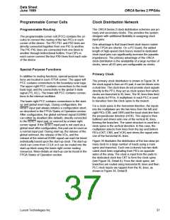
Programmable Corner Cells
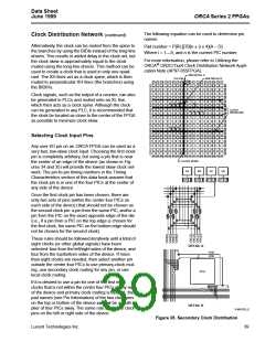
Clock Distribution Network
The ORCA Series 2 clock distribution schemes use pri-
mary and secondary clocks. This provides the system
designer with additional flexibility in assigning clock
input pins.
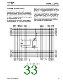
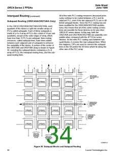
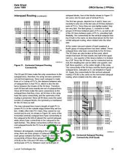
Programmable Routing
The programmable corner cell (PCC) contains the cir-
cuitry to connect the routing of the two PICs in each
corner of the device. The PIC PX1 and PX2 lines are
directly connected together from one PIC to another.
The PIC PXL lines are connected from one block to
another through tridirectional buffers. Four CIPs in
each corner connect the four PXH lines from each side
of the device.
One advantage is that board-level clock traces routed
to the FPGA are shorter. On a PC board, the added
length of high-speed clock traces routed to dedicated
clock input pins can significantly increase the parasitic
impedances. The primary advantage of the ORCA
clock distribution is the availability of a large number of
clocks, since all I/O pins are configurable as clocks.
Special-Purpose Functions
Primary Clock
In addition to routing functions, special-purpose func-
tions are located in each FPGA corner. The upper-left
PCC contains connections to the boundary-scan logic.
The upper-right PCC contains connections to the read-
back logic and the connectivity to the global 3-state
signal (TS_ALL). The lower-left PCC contains connec-
tions to the internal oscillator.
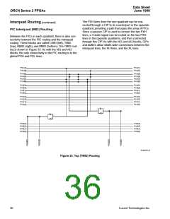
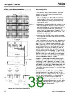
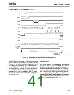
The primary clock distribution is shown in Figure 34. If
the clock signal is from an I/O pad, it can be driven onto
a clock line. The clock lines do not provide clock signals
directly to the PFU; they act as clock spines from which
clocks are branched to XL lines. The XL lines then feed
the clocks to PFUs. A multiplexer in each PLC is used
to transition from the clock spine to the branch.
The lower-right PCC contains connections to the start-
up and global reset logic. During configuration, the
RESET input pad always initiates a configuration abort,
as described in the FPGA States of Operation section.
After configuration, the global set/reset signal (GSRN)
can either be disabled (the default), directly connected
to the RESET input pad, or sourced by a lower-right
corner signal. If the RESET input pad is not used as a
global reset after configuration, this pad can be used as
a normal input pad. During start-up, the release of the
global set/reset, the release of the I/Os, and the
release of the external DONE signal can each be timed
individually based upon the start-up clock. The start-up
clock can come from CCLK or it can be routed into the
start-up block using the lower-right corner routing
resources. More details on start-up can be found in the
FPGA States of Operation section.
For a clock spine in the horizontal direction, the inputs
into the multiplexer are the two lines from the left and
right PICs (CKL and CKR) and the local clock line from
the perpendicular direction (HCK). This signal is then
buffered and driven onto one of the vertical XL lines,
forming the branches. The same structure is used for a
clock spine in the vertical direction. In this case, the
multiplexer selects from lines from the top and bottom
PICs (CKT, CKB, and VCK) and drives the signal onto
one of the horizontal XL lines.
Figure 34 illustrates the distribution of the low-skew pri-
mary clock to a large number of loads using a main
spine and branches. Each row (column) has two dedi-
cated clock lines originating from PICs on opposite
sides of the array. The clock is input from the pads to
the dedicated clock line CKT to form the clock spine
(see Figure 34, Detail A). From the clock spine, net
branches are routed using horizontal XL lines and then
PLC clock inputs are tapped from the XL lines, as
shown in Figure 34, Detail B.
Lucent Technologies Inc.
37

 ETC [ ETC ]