Data Sheet
June 1999
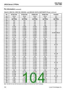
ORCA Series 2 FPGAs
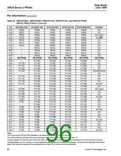
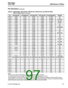
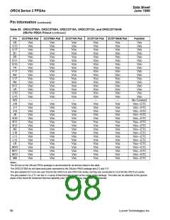
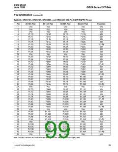
Pin Information (continued)
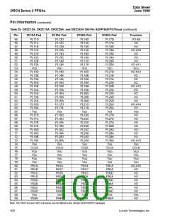
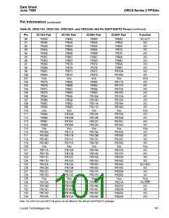
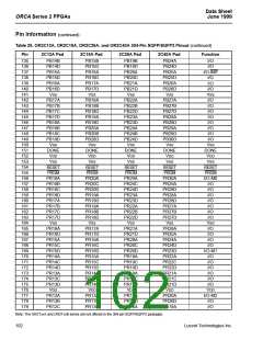
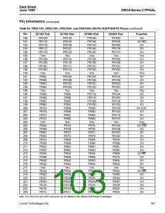
Table 26. OR2C12A, OR2C15A, OR2C26A, and OR2C40A 304-Pin SQFP/SQFP2 Pinout (continued)
Pin
2C12A Pad
2C15A Pad
2C26A Pad
2C40A Pad
Function
45
46
47
48
49
50
51
52
53
54
55
56
57
58
59
60
61
62
63
64
65
66
67
68
69
70
71
72
73
74
75
76
77
78
79
80
81
82
83
84
85
86
87
88
89
PL11D
PL11C
PL11B
PL11A
PL12D
PL12C
PL12B
PL12A
VDD
PL13D
PL13B
PL13A
PL14D
PL14B
PL14A
PL15D
PL15B
PL15A
PL16D
PL16A
VSS
PL17D
PL17C
PL17B
PL17A
PL18D
PL18C
PL18B
PL18A
VSS
CCLK
VDD
VSS
VDD
VSS
PB1A
PB1B
PB1C
PB1D
PB2A
PB2B
PB2C
PB2D
VSS
PL12D
PL12C
PL12B
PL12A
PL13D
PL13C
PL13B
PL13A
VDD
PL14D
PL14B
PL14A
PL15D
PL15B
PL15A
PL16D
PL16B
PL16A
PL17D
PL17A
VSS
PL18D
PL18C
PL18A
PL19D
PL19C
PL19A
PL20D
PL20A
VSS
CCLK
VDD
VSS
VDD
VSS
PB1A
PB1C
PB1D
PB2A
PB2D
PB3A
PB3C
PB3D
VSS
PL14D
PL14A
PL15D
PL15A
PL16D
PL16A
PL17D
PL17A
VDD
PL18D
PL18B
PL18A
PL19D
PL19B
PL19A
PL20D
PL20B
PL20A
PL21D
PL21A
VSS
PL22D
PL22C
PL22A
PL23D
PL23C
PL23A
PL24D
PL24A
VSS
CCLK
VDD
VSS
VDD
VSS
PB1A
PB1C
PB1D
PB2A
PB2D
PB3A
PB3C
PB3D
VSS
PL17D
PL17A
PL18D
PL18A
PL19D
PL19A
PL20D
PL20A
VDD
PL21D
PL21B
PL21A
PL22D
PL22B
PL22A
PL23D
PL24D
PL25D
PL25A
PL26A
VSS
PL27D
PL27C
PL27A
PL28D
PL28C
PL28A
PL29A
PL30A
VSS
CCLK
VDD
VSS
VDD
VSS
PB1A
PB2A
PB2D
PB3A
PB3D
PB4A
PB4C
PB4D
VSS
I/O-A9
I/O
I/O
I/O-A10
I/O
I/O
I/O
I/O-A11
VDD
I/O-A12
I/O
I/O
I/O
I/O-A13
I/O
I/O
I/O
I/O
I/O-A14
I/O
VSS
I/O
I/O
I/O
I/O
I/O
I/O
I/O
I/O-A15
VSS
CCLK
VDD
VSS
VDD
VSS
I/O-A16
I/O
I/O
I/O
I/O
I/O
I/O
I/O
VSS
I/O
PB3A
PB4A
PB4A
PB5A
Note: The OR2TxxA and OR2TxxB series are not offered in the 304-pin SQFP/SQFP2 packages.
100
Lucent Technologies Inc.

 ETC [ ETC ]