一華半導體股份有限公司
PIR CONTROLLER
MOSDESIGN SEMICONDUCTOR CORP.
DC PIR CONTROLLER
M7613
WITH REMOTE CONTROL
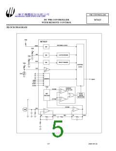
PIN DESCRIPTION
Pin No.
Pin Name
A0~A3
I/O
I
Description
18 Pins 20 Pins
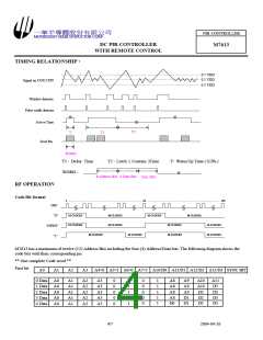
Code Address pin Nos.0~3. There four tri-state pins are detected to determine
the encoded waveform bit 0 ~ bit 3.Each pin can be set to “0”,”1” or
“f”(floating).
1-4
5-6
1-4
5-8
Code Address pin Nos.8~11/Data pin Nos.0~3.
There four tri-state pins are detected to determine the encoded waveform bit 8 ~
bit 11.When these pins are used as address pins, they can be set to “0”,”1” or
“f”(floating).When these pins are used as data pins, they can be set only to
“0”ot”1”.
A8/D0~A11/D3
I
Rosc
VSS
CDS
I
I
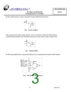
Encoder system oscillator ( Rosc=1.1Mohm,Typ.=38KHz )
System ground.
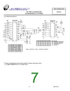
7
8
9
9
10
11
Connect to a CDS for inhibit , when Vinhi = 0 disable ,Vinhi = 1 enable trigger
Delay timer oscillator input
The delay time of receiving PIR signal to trigger Encoder or a high signal to
trigger relay.
The range for:RTX=2 KΩ ~ 5 MΩ
CTX=100P~0.01UF
RTX
I
FOR 100P or 0.01uf delay time=45000 R*C
FOR 1000P delay time=35000 R*C
Delay Time :20 ms ~ 2250s
10
12
Ex:CTX=100p,RTX=680KΩ,Delay Time=3.1s
CTX=1000p,RTX=100KΩ,Delay Time=3.5s
CTX=0.01uf,RTX=10KΩ,Delay Time=4.5s
Latch timer oscillator input
The latch time ofthe range for:RTI=100 KΩ ~ 1 MΩ
CTI=0.1UF(fix)
RTI
I
11
13
Contain Time=35 R*C
Contain time :> 0.5s ~
Ex:CTI=0.1uf,RTI=1MΩ,Contain Time=3.5s
UOU2
II2
O
I
2nd stage OP amp output.
12
13
14
15
16
14
15
16
17
18
2nd stage OP amp negative input.
1st stage OP amp positive input.
1st stage OP amp negative input.
1st stage OP amp output.
NII1
II1
I
I
UOU1
I
Data Output pin. The encoder waveform is serially outputted to this pin.
DOUT
VDD
O
17
18
19
20
When PIR is not detecting,DOUT output low (VSS) voltage
Operation voltage:5V,Stand by current:80~90uA
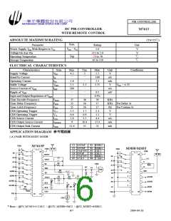
2/7
2004-04-26

 ETC [ ETC ]