MAX 3000A Programmable Logic Device Family Data Sheet
Programmable Interconnect Array
Logic is routed between LABs on the PIA. This global bus is a
programmable path that connects any signal source to any destination on
the device. All MAX 3000A dedicated inputs, I/O pins, and macrocell
outputs feed the PIA, which makes the signals available throughout the
entire device. Only the signals required by each LAB are actually routed
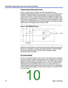
from the PIA into the LAB. Figure 5 shows how the PIA signals are routed
into the LAB. An EEPROM cell controls one input to a two-input ANDgate,
which selects a PIA signal to drive into the LAB.
Figure 5. MAX 3000A PIA Routing
To LAB
PIA Signals
While the routing delays of channel–based routing schemes in masked or
FPGAs are cumulative, variable, and path–dependent, the MAX 3000A
PIA has a predictable delay. The PIA makes a design’s timing
performance easy to predict.
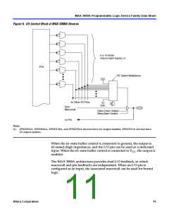
I/O Control Blocks
The I/O control block allows each I/O pin to be individually configured
for input, output, or bidirectional operation. All I/O pins have a tri–state
buffer that is individually controlled by one of the global output enable
signals or directly connected to ground or VCC. Figure 6 shows the I/O
control block for MAX 3000A devices. The I/O control block has 6 or
10 global output enable signals that are driven by the true or complement
of two output enable signals, a subset of the I/O pins, or a subset of the
I/O macrocells.
10
Altera Corporation

 ETC [ ETC ]