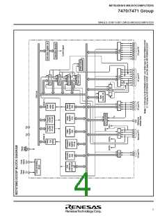
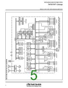
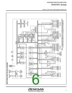
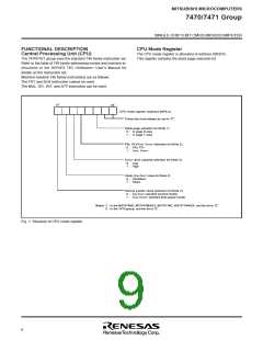
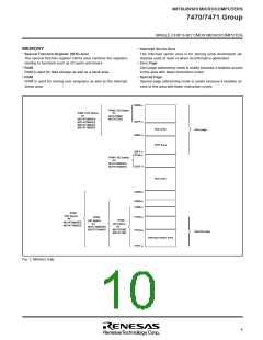
MITSUBISHI MICROCOMPUTERS
7470/7471 Group
SINGLE-CHIP 8-BIT CMOS MICROCOMPUTER
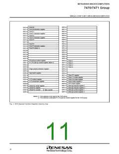
PIN DESCRIPTION
Input/
Output
Pin
Name
Functions
Apply voltage of 2.7 to 5.5 V to VCC, and 0 V to VSS.
Power source voltage
VCC, VSS
Analog power
source
AVSS
(Note 1)
Ground level input pin for A-D converter.
Same voltage as VSS is applied.
Reset input
Input
RESET
To enter the reset state, the reset input pin must be kept at “L” for 2 µs or more
(under normal VCC conditions).
Clock input
Input
XIN
These are I/O pins of internal clock generating circuit for main clock. To control
generating frequency, an external ceramic or a quartz-crystal oscillator is
connected between the XIN and XOUT pins. If an external clock is used, the
clock source should be connected the XIN pin and the XOUT pin should be left
open. Feedback resistor is connected between XIN and XOUT.
Clock output
Output
XOUT
Reference voltage
input
Input
I/O
VREF
Reference voltage input pin for the A-D converter.
I/O port P0
P00–P07
Port P0 is an 8-bit I/O port. The output structure is CMOS output.
When this port is selected for input, pull-up transistor can be connected in
units of 1-bit and a key on wake up function is provided.
I/O port P1
I/O
P10–P17
Port P1 is an 8-bit I/O port. The output structure is CMOS output.
When this port is selected for input, pull-up transistor can be connected in
units of 4-bit. P12, P13 are in common with timer output pins T0, T1, P14, P15,
P16, P17 are in common with serial I/O pins SIN, SOUT, CLK, SRDY, respec-
tively. The output structure of SOUT and SRDY can be changed to N-channel
open drain output.
I/O port P2
I/O
P20–P27
(Note 2)
Port P2 is an 8-bit I/O port. The output structure is CMOS output.
When this port is selected for input, pull-up transistor can be connected in
units of 4-bit.
This port is in common with analog input pins IN0–IN7.
Input port P3
Input
P30–P33
Port P3 is a 4-bit input port. P30, P31 are in common with external interrupt
input pins INT0, INT1, and P32, P33 are in common with timer input pins
CNTR0, CNTR1.
I/O port P4
I/O
P40–P43
(Note 3)
Port P4 is a 4-bit I/O port. The output structure is CMOS output. When this
port is selected for input, pull-up transistor can be connected in units of 4-bit.
Input port P5
Input
P50–P53
(Note 4)
Port P5 is a 4-bit input port and pull-up transistor can be connected in units of
4-bit. P50, P51 are in common with input/output pins of clock for clock function
XCIN, XCOUT. When P50, P51 are used as XCIN, XCOUT, connect a ceramic or a
quartz-crystal oscillator between XCIN and XCOUT.
If an external clock input is used, connect the clock input to the XCIN pin and
open the XCOUT pin. Feedback resistor is connected between XCIN and XCOUT
pins.
Notes 1 : AVSS for M37471M2/M4/M8/E4/E8-XXXFP.
2 : Only P20–P23 (IN0–IN3) 4-bit for 7470 group.
3 : Only P40 and P41 2-bit for 7470 group.
4 : This port is not included in 7470 group.
7

 ETC [ ETC ]