Chapter 3 Scan Path Block
Chapter 3 Scan Path Block
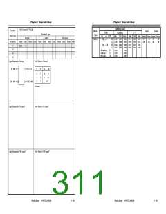
Switching speed
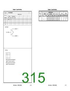
Clock Distributor
Function
Block
type
Input
Output
Path
→
t LD0 (ns)
t 1
Standard type
Block type
IN
CL
OUT
MIN.
(HH) 0.215
(LL) 0.224
(HH) 0.214
(LL) 0.223
TYP. MAX.
MIN.
0.011
0.010
0.011
0.010
TYP. MAX. Symbol Fanin Symbol Fanout
Normal
High speed
Name cells
0.327
0.365
0.326
0.364
0.590
0.684
0.589
0.683
0.015
0.013
0.015
0.013
0.022
0.019
0.022
0.019
CL
2.1
Y
Z
34
34
SCD1
→
Y
Z
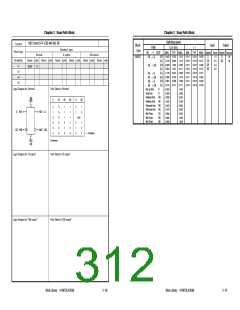
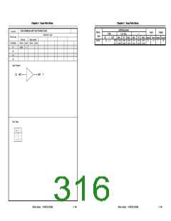
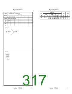
Drivability
Name cells
CL
→
SCD1
8
x1
x2
x4
x8
Logic Diagram
N01
N02
Y
Z
CL H01
Truth Table
CL
Y
Z
1
0
1
0
1
0
Y:Must be connected to the clock of Negative edge
triggered F/F or the gate of Low enable Latch
Z:Must be connected to the clock of Positice edge
triggered F/F or the gate of High enable Latch
Block Library A13872EJ5V0BL
3 - 66
Block Library A13872EJ5V0BL
3 - 67

 ETC [ ETC ]