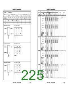
Chapter 2 Function Block
Chapter 2 Function Block
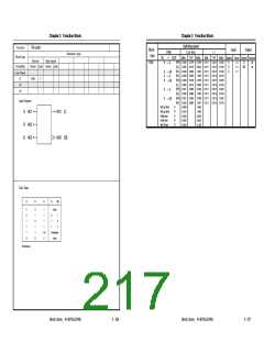
Switching speed
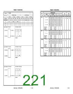
D-Latch
Function
Block
type
Input
Output
Path
→
t LD0 (ns)
t 1
Standard type
Low Gate type
Block type
IN
OUT
MIN.
(HH) 0.432
(LL) 0.436
(HL) 0.340
(LH) 0.310
(HH) 0.476
(HL) 0.480
(HH) 0.354
(HL) 0.385
0.600
TYP. MAX.
MIN.
0.012
0.010
0.010
0.012
0.012
0.010
0.012
0.010
TYP. MAX. Symbol Fanin Symbol Fanout
Normal
Q output
QB output
Normal
Q output
QB output
0.699
0.738
0.536
0.521
0.790
0.774
0.558
0.629
1.319
1.415
0.987
0.995
1.505
1.427
1.009
1.174
1.000
0.010
1.836
0.696
0.816
0.870
0.862
1.010
0.100
1.195
0.765
0.901
0.949
0.978
1.080
0.050
1.316
0.984
0.990
1.012
1.172
0.970
0.070
1.501
0.016
0.013
0.013
0.016
0.016
0.013
0.016
0.013
0.022
0.017
0.017
0.022
0.022
0.017
0.022
0.017
D
G
1.0
1.0
Q
32
32
F601
D
D
G
G
→
→
→
→
Q
Drivability
Name cells
Name cells
Name cells
Name cells
Name cells
Name cells
QB
QB
Q
Low Power
L601
4
F601
6
F601NQ
5
F601NB
5
x1
x2
x4
QB
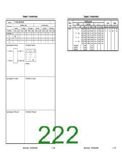
Logic Diagram for "Normal"
Truth Table for "Normal"
Set up time
Hold time
Min Pulse
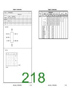
D
D
G
0.250
0.639
(HH) 0.251
D
G
Q
QB
D
G
H01
H02
N01
Q
0.383
0.430
0.467
0.478
0.022
0.021
0.022
0.021
0.030
0.027
0.030
0.027
0.043
0.037
0.043
0.037
D
G
1.0
1.0
Q
Q
16
31
32
L601
D
→
Q
(LL)
0.260
0
1
X
1
1
0
0
1
1
0
(HH) 0.288
(HL) 0.295
0.600
0.270
0.450
(HH) 0.271
G
→
Q
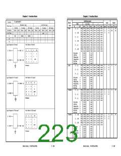
Latch
Set up time
Hold time
Min Pulse
D
D
G
N02 QB
X:Irrelevant
0.416
0.470
0.508
0.529
0.012
0.011
0.012
0.011
0.016
0.014
0.016
0.014
0.023
0.019
0.023
0.019
D
G
1.0
1.0
F601NQ
F601NB
D
→
Q
(LL)
0.280
(HH) 0.313
(HL) 0.323
0.610
G
→
Q
Set up time
Hold time
Min Pulse
D
D
G
0.260
0.480
Logic Diagram for "Q output"
Truth Table for "Q output"
(HL) 0.337
(LH) 0.306
(HH) 0.353
(HL) 0.383
0.590
0.534
0.517
0.558
0.628
0.010
0.012
0.012
0.010
0.013
0.016
0.016
0.013
0.017
0.022
0.022
0.017
D
G
1.0
1.0
QB
D
→
QB
D
G
Q
D
H01
N01
Q
G
→
QB
0
1
X
1
1
0
0
1
Set up time
Hold time
Min Pulse
D
D
G
0.280
0.516
Latch
G
H02
X:Irrelevant
Logic Diagram for "QB output"
Truth Table for "QB output"
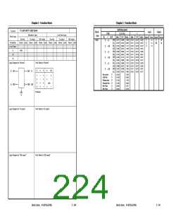
D
G
QB
D
H01
0
1
X
1
1
0
1
0
Latch
G
H02
N01 QB
X:Irrelevant
Block Library A13872EJ5V0BL
2 - 234
Block Library A13872EJ5V0BL
2 - 235

 ETC [ ETC ]