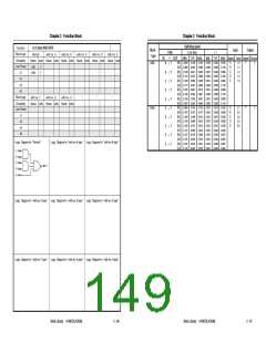
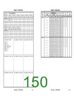
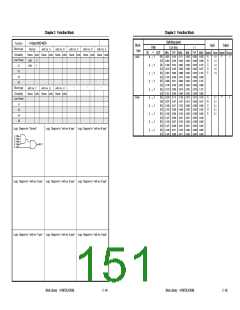
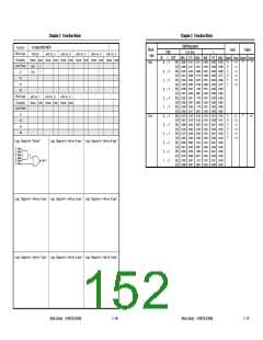
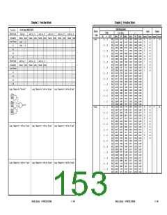
Chapter 2 Function Block
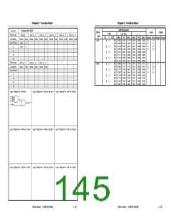
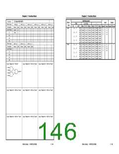
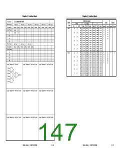
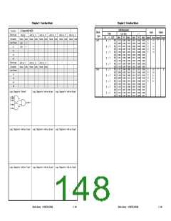
1-2-2-Input AND-NOR
Chapter 2 Function Block
Switching speed
Function
Block type
Drivability
Low Power
x1
Block
type
Input
Output
Path
→
t LD0 (ns)
t 1
Normal
with inv. A
with inv. B
with inv. C
with inv. D
with inv. E
IN
OUT
MIN.
TYP. MAX.
MIN.
0.020
0.038
0.031
0.050
0.031
0.048
0.031
0.048
0.031
0.050
0.010
0.022
0.015
0.027
0.015
0.027
0.016
0.027
0.016
0.027
TYP. MAX. Symbol Fanin Symbol Fanout
Name cells
Name cells
Name cells
Name cells
Name cells
Name cells
(HL) 0.094
(LH) 0.093
(HL) 0.146
(LH) 0.113
(HL) 0.133
(LH) 0.171
(HL) 0.167
(LH) 0.145
(HL) 0.150
(LH) 0.207
(HL) 0.084
(LH) 0.107
(HL) 0.123
(LH) 0.142
(HL) 0.123
(LH) 0.141
(HL) 0.137
(LH) 0.175
(HL) 0.137
(LH) 0.175
0.146
0.343
0.241
0.375
0.233
0.457
0.291
0.455
0.279
0.554
0.124
0.197
0.196
0.299
0.197
0.300
0.219
0.405
0.216
0.404
0.184
0.293
0.426
0.596
0.408
0.656
0.512
0.851
0.491
0.929
0.145
0.147
0.314
0.457
0.314
0.455
0.348
0.730
0.347
0.730
0.024
0.082
0.042
0.087
0.042
0.082
0.043
0.082
0.043
0.082
0.012
0.043
0.021
0.044
0.021
0.044
0.022
0.044
0.022
0.044
0.032
0.118
0.064
0.123
0.064
0.118
0.069
0.119
0.069
0.118
0.016
0.060
0.033
0.063
0.033
0.063
0.037
0.063
0.037
0.063
A
B
C
D
E
1.0
1.0
1.0
1.0
1.0
Y
2
L428
A
B
C
D
E
A
B
C
D
E
→
→
→
→
→
→
→
→
→
→
Y
Y
Y
Y
Y
Y
Y
Y
Y
Y
L428
F428
3
5
x2
x4
x8
-
-
-
Block type
with inv. F
with inv. G
with inv. H
Drivability
Name cells
Name cells
Name cells
A
B
C
D
E
2.1
2.0
2.0
2.0
2.0
Y
7
F428
Low Power
x1
x2
x4
x8
Logic Diagram for "Normal"
Logic Diagram for "with inv. A type"
Logic Diagram for "with inv. D type"
Logic Diagram for "with inv. G type"
Logic Diagram for "with inv. B type"
Logic Diagram for "with inv. E type"
Logic Diagram for "with inv. H type"
E
D
C
B
A
H05
H04
H03
H02
H01
N01 Y
Logic Diagram for "with inv. C type"
Logic Diagram for "with inv. F type"
Block Library A13872EJ5V0BL
2 - 90
Block Library A13872EJ5V0BL
2 - 91

 ETC [ ETC ]