Chapter 2 Function Block
Chapter 2 Function Block
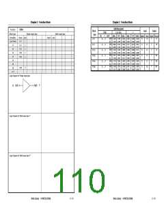
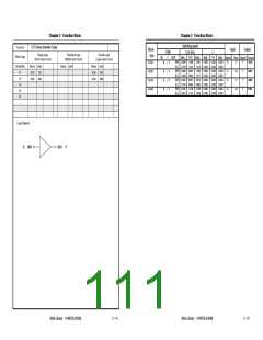
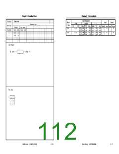
Switching speed
Buffer
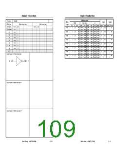
Function
Block
type
Input
Output
Path
→
t LD0 (ns)
t 1
Block type
Single output type
Multi output type
IN
OUT
MIN.
(HH) 0.128
(LL) 0.126
(HH) 0.095
(LL) 0.099
(HH) 0.126
(LL) 0.129
(HH) 0.151
(LL) 0.159
(HH) 0.175
(LL) 0.183
(HH) 0.148
(LL) 0.151
TYP. MAX.
MIN.
0.022
0.020
0.011
0.010
0.006
0.005
0.004
0.003
0.003
0.003
0.001
0.001
TYP. MAX. Symbol Fanin Symbol Fanout
Drivability
Name cells
Name cells
0.196
0.198
0.144
0.149
0.182
0.194
0.216
0.237
0.245
0.276
0.210
0.226
0.334
0.356
0.243
0.259
0.296
0.333
0.350
0.413
0.396
0.482
0.336
0.389
0.030
0.024
0.015
0.012
0.008
0.006
0.005
0.004
0.004
0.003
0.002
0.002
0.042
0.033
0.021
0.016
0.011
0.008
0.007
0.006
0.005
0.004
0.003
0.002
A
A
A
A
A
A
1.0
2.1
2.1
2.1
2.1
6.2
Y
Y
Y
Y
Y
Y
17
35
L111
F111
F112
F153
F154
F158
A
A
A
A
A
A
→
→
→
→
→
→
Y
Y
Y
Y
Y
Y
Low Power
L111
1
x1
x2
F111
F112
2
3
70
x3
F153
F154
4
5
104
139
278
x4
x5
x6
F158
11
x8
x12
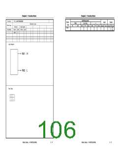
Logic Diagram for "Single output type"
A
H01
N01
Y
Logic Diagram for "Multi output type 1"
Logic Diagram for "Multi output type 2"
Block Library A13872EJ5V0BL
2 - 12
Block Library A13872EJ5V0BL
2 - 13

 ETC [ ETC ]