RT9167/A
Current Limit and Thermal Protection
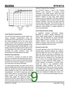
The RT9167 includes a current limit which monitors
and controls the pass transistor’s gate voltage limiting
the output current to 300mA Typ. (700mA Typ. for
RT9167A). Thermal-overload protection limits total
power dissipation in the RT9167/A. When the junction
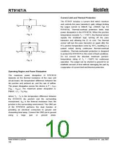
V
V
IN
OUT
Fig. 3
temperature exceeds T = +155°C, the thermal sensor
J
signals the shutdown logic turning off the pass
transistor and allowing the IC to cool. The thermal
sensor will turn the pass transistor on again after the
IC’s junction temperature cools by 10°C, resulting in a
pulsed output during continuous thermal-overload
conditions. Thermal-overloaded protection is designed
to protect the RT9167/A in the event of fault conditions.
Do not exceed the absolute maximum junction-
V
V
IN
OUT
temperature rating of T = +150°C for continuous
J
Fig. 4
operation. The output can be shorted to ground for an
indefinite amount of time without damaging the part by
cooperation of current limit and thermal protection.
Operating Region and Power Dissipation
The maximum power dissipation of RT9167/A
depends on the thermal resistance of the case and
circuit board, the temperature difference between the
die junction and ambient air, and the rate of airflow.
The power dissipation across the device is P = I
OUT
(V - V
). The maximum power dissipation is:
IN
OUT
PMAX = (T - T ) /θ
J
A
JA
where T - T is the temperature difference between
J
A
the RT9167/A die junction and the surrounding
environment, θ is the thermal resistance from the
JA
junction to the surrounding environment. The GND pin
of the RT9167/A performs the dual function of
providing an electrical connection to ground and
channeling heat away. Connect the GND pin to ground
using
a
large
pad
or
ground
plane.
www.richtek-ic.com.tw
DS9167/A-10 July 2001
10

 ETC [ ETC ]