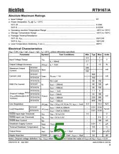
RT9167/A
Internal P-Channel Pass Transistor
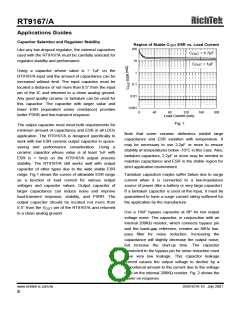
C
= 1nF
BP
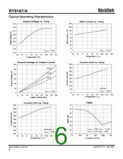
The RT9167/A features a typical 1.1Ω P-channel
MOSFET pass transistor. It provides several
advantages over similar designs using PNP pass
transistors, including longer battery life. The P-channel
MOSFET requires no base drive, which reduces
quiescent current considerably. PNP-based regulators
waste considerable current in dropout when the pass
transistor saturates. They also use high base-drive
currents under large loads. The RT9167/A does not
suffer from these problems and consume only 80µA of
quiescent current whether in dropout, light-load, or
heavy-load applications.
C
= 10nF
BP
V
= 3.0V
OUT
0
5.0
10.0
15.0
Fig. 2
Input-Output (Dropout) Voltage
A
regulator’s minimum input-output voltage
Load-Transient Considerations
differential (or dropout voltage) determines the
lowest usable supply voltage. In battery-powered
systems, this will determine the useful end-of-life
battery voltage. Because the RT9167/A uses a P-
channel MOSFET pass transistor, the dropout
voltage is a function of drain-to-source on-resistance
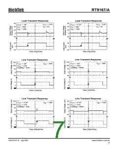
The RT9167/A load-transient response graphs (see
Typical Operating Characteristics) show two
components of the output response: a DC shift from
the output impedance due to the load current
change, and the transient response. The DC shift is
quite small due to the excellent load regulation of the
IC. Typical output voltage transient spike for a step
change in the load current from 0mA to 50mA is tens
mV, depending on the ESR of the output capacitor.
Increasing the output capacitor’s value and
decreasing the ESR attenuates the overshoot.
[R
] multiplied by the load current.
DS(ON)
Reverse Current Path
The power transistor used in the RT9167/A has an
inherent diode connected between the regulator
input and output (see Fig.3). If the output is forced
above the input by more than a diode-drop, this
diode will become forward biased and current will
Shutdown Input Operation
The RT9167/A is shutdown by pulling the SHDN
input low, and turned on by driving the input high. If
this feature is not to be used, the SHDN input should
be tied to VIN to keep the regulator on at all times
(the SHDN input must not be left floating).
flow from the V
terminal to V . This diode will
OUT
IN
also be turned on by abruptly stepping the input
voltage to a value below the output voltage. To
prevent regulator mis-operation, a Schottky diode
should be used in any applications where
input/output voltage conditions can cause the
internal diode to be turned on (see Fig.4). As shown,
the Schottky diode is connected in parallel with the
internal parasitic diode and prevents it from being
turned on by limiting the voltage drop across it to
about 0.3V. < 100 mA to prevent damage to the part.
To ensure proper operation, the signal source used to
drive the SHDN input must be able to swing above and
below the specified turn-on/turn-off voltage thresholds
which guarantee an ON or OFF state (see Electrical
Characteristics). The ON/OFF signal may come from
either CMOS output, or an open-collector output with
pull-up resistor to the RT9167/A input voltage or
another logic supply. The high-level voltage may
exceed the RT9167/A input voltage, but must remain
within the absolute maximum ratings for the SHDN pin.
DS9167/A-10 July 2001
www.richtek-ic.com.tw
9

 ETC [ ETC ]