8.14
Input/Output Data Inversion Function
8.14.1
Overview
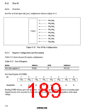
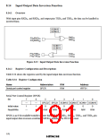
With input pins RXD31, and RXD32, and output pins TXD31 and TXD32, the data can be handled in
inverted form.
SCINV0
SCINV2
RXD31
RXD32
P34/RXD31
P41/RXD32
SCINV1
SCINV3
P35/TXD31
P42/TXD32
TXD31
TXD32
Figure 8.13 Input/Output Data Inversion Function
Register Configuration and Descriptions
8.14.2
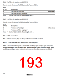
Table 8.34 shows the registers used by the input/output data inversion function.
Table 8.34 Register Configuration
Name
Abbreviation
R/W
Address
Serial port control register
SPCR
R/W
H'FF91
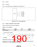
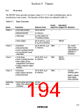
Serial Port Control Register (SPCR)
Bit
7
—
1
6
—
1
5
4
3
2
1
0
SPC32 SPC31 SCINV3 SCINV2 SCINV1 SCINV0
Initial value
Read/Write
0
0
0
0
0
0
—
—
R/W
R/W
R/W
R/W
R/W
R/W
SPCR is an 8-bit readable/writable register that performs RXD31, RXD32, TXD31, and TXD32 pin
input/output data inversion switching. SPCR is initialized to H'C0 by a reset.
176

 ETC [ ETC ]