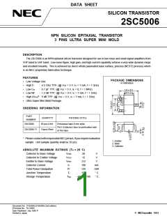
2SC5006
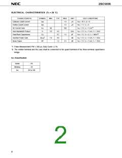
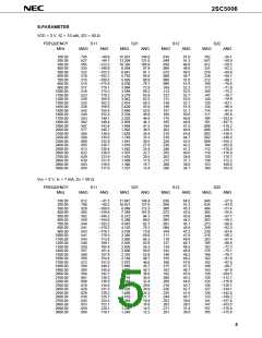
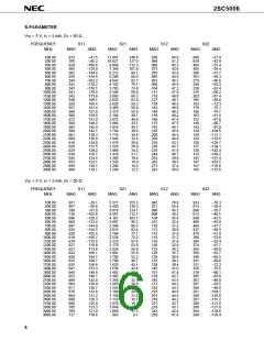
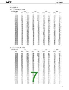
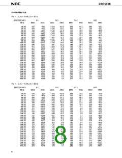
ELECTRICAL CHARACTERISTICS (TA = 25 ˚C)
CHARACTERISTIC
Collector Cutoff Current
Emitter Cutoff Current
DC Current Gain
SYMBOL
ICBO
IEBO
MIN.
TYP.
MAX.
1.0
UNIT
µA
TEST CONDITIONS
VCB = 10 V, IE = 0
1.0
µA
VEB = 1 V, IC = 0
*1
hFE
80
160
VCE = 3 V, IC = 7 mA
Gain Bandwidth Product
Feed-Back Capacitance
Insertion Power Gain
Noise Figure
fT
3.0
4.5
0.7
9.0
1.2
GHz
pF
VCE = 3 V, IC = 7 mA, f = 1 GHz
*2
Cre
1.5
2.5
VCB = 3 V, IE = 0, f = 1 MHz
2
|S21e|
7.0
dB
VCE = 3 V, IC = 7 mA, f = 1 GHz
VCE = 3 V, IC = 7 mA, f = 1 GHz
NF
dB
*1 Pulse Measurement PW ≤ 350 µs, Duty Cycle ≤ 2 %
*2 The emitter terminal and the case shall be connected to the guard terminal of the three-terminal capacitance
bridge.
hFE Classification
RANK
Marking
hFE
FB
24
80 to 160
2
图片预览")
 ETC [ ETC ]