PRELIMINARY
PCT1789W DATA SHEET
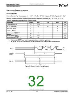
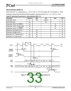
SWITCHING CHARACTERISTICS
!!
Serial Interface (DCE = 0)
Given values are: VA = charge pump, VD = +3.3 V ± 5%; TA = 70 °C for K-grade, 85 °C for B-grade; CL = 20 pF.
All timing is referenced to the 50% level of the waveform. Input test levels are: VIH = VD – 0.4V, VIL = 0.4V.
Table 25 Switching Characteristics—Serial Interface (DCE = 0)
Parameter
Symbol
Min
Typ
Max
Unit
Cycle time, SCLK
tc
354
1/256 Fs
ns
SCLK duty cycle
tdty
td1
td2
td3
tsu
th
50
%
ns
ns
ns
ns
ns
ns
ns
Delay time, SCLK • to FSYNC ¯
Delay time, SCLK • to SDO valid
Delay time, SCLK • to FSYNC •
Setup time, SDI before SCLK ¯
Hold time, SDI after SCLK ¯
Setup time, FC • before SCLK •
Hold time, FC • after SCLK •
10
20
10
25
20
40
40
tsfc
thfc
tc
VOH
VOL
SCLK
td3
td1
FSYNC
(mode 0)
td3
FSYNC
(mode 1)
td2
16-bit
SDO
D15
tsu
D14
... D2
D1
D0
th
16-bit
SDI
D15
D14
... D2
D1
D0
tsfc
thfc
FC
Figure 17 Serial Interface Timing Diagram (DCE = 0)
PRELIMINARY
PC-TEL, Inc.
56
1789W0DOCDAT06A-0299

 ETC [ ETC ]