PCT2303N DATA SHEET
AC-LINK CHARACTERISTICS
!!
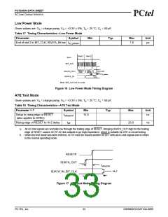
Low Power Mode
Given values are: VA = charge pump, VD = +3.3V ± 5%; TA = 25 °C; CL = 50 pF.
Table 17 Timing Characteristics—Low Power Mode
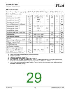
Parameter
Symbol
Min
Typ
Max
Unit
End of slot 2 to BIT_CLK, SDATA_IN low ts2_pdown
1.0
µs
Slot 1 Slot 2
Sync
BIT_CLK
Data
MLNK
Write to
0x56
Don’t care
SDATA_OUT
SDATA_IN
t
s2_pdown
Note: BIT_CLK not to scale
Figure 16 Low Power Mode Timing Diagram
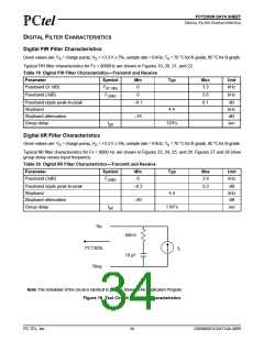
ATE Test Mode
Given values are: VA = charge pump, VD = +3.3V ± 5%; TA = 25 °C; CL = 50 pF.
Table 18 Timing Characteristics—ATE Test Mode
Parameter a, b
Symbol
Min
Typ
Max
Unit
Setup to rising edge of RESET
(also applies to SYNC)
tsetup2rst
15.0
ns
Rising edge of RESET to Hi-Z delay
toff
25.0
ns
a. All AC-link signals are normally low through the trailing edge of RESET. Bringing SDATA_OUT high for the trailing
edge of RESET causes AC’97 AC-link outputs to go high impedance, which is suitable for ATE in circuit testing.
b. When the test mode has been entered, AC’97 must be issued another RESET with all AC-link signals low to return
to the normal operating mode.
RESET#
SDATA_OUT
tsetup2rst
Hi-Z
SDATA_IN, BIT_CLK
toff
Figure 17 ATE Test Mode Timing Diagram
PC-TEL, Inc.
33
2303N0DOCDAT10A-0899

 ETC [ ETC ]