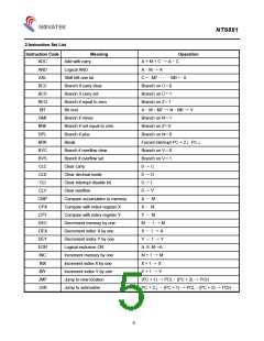
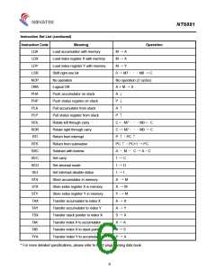
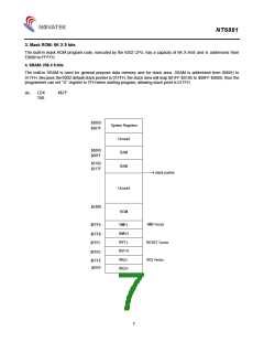
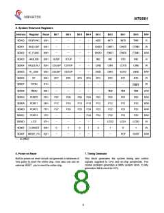
NT6881
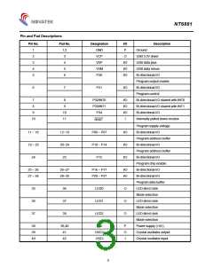
Pin and Pad Descriptions
Pin No.
Pad No.
Designation
GND
I/O
P
Description
1
2
3
4
5
1,2
3
Ground
VCP
O
USB 3.3V driver
USB data plus
4
VDP
I/O
I/O
I/O
5
VDM
USB data minus
Bi-directional I/O
Program output enable
Bi-directional I/O
Program control
6
P30
6
7
P31
I/O
7
8
8
9
P32/INT0
P33/INT1
P34
I/O
I/O
I/O
I
Bi-directional I/O shared with INT0
Bi-directional I/O shared with INT1
Bi-directional I/O
9
10
11
10
Internally pulled down resistor
RESET
P00 ~ P07
P10 ~ P14
P15
Program supply voltage
Bi-directional I/O
11 ~ 18
19 ~ 23
24
12~19
20~24
25
I/O
I/O
I/O
Program address buffer
Bi-directional I/O
Program address buffer
Bi-directional I/O
Program chip enable
Bi-directional I/O
25 ~ 26
27 ~ 34
26~27
28~35
P16 ~ P17
P20 ~ P27
I/O
I/O
Bi-directional I/O
Program data buffer
LED direct sink
35
36
37
36
37
38
LED0
LED1
LED2
O
O
O
Mode selection
LED direct sink
Mode selection
LED direct sink
Mode selection
38
39
40
39,40
41
VDD
P
O
I
Power supply (+5V)
Crystal oscillator output
Crystal oscillator input
OSCO
OSCI
42
3

 ETC [ ETC ]