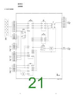
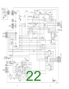
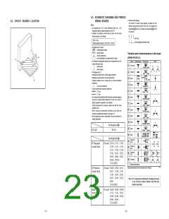
5-3. SCHEMATIC DIAGRAMS AND PRINTED
•
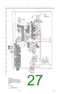
Divided circuit diagram
WIRING BOARDS
5-2. CIRCUIT BOARDS LOCATION
One sheet of D board circuit diagram is divided into four
sheets, each having the code D-a to D-d . For example, the
destination ab1 on the D-a sheet is connected to ab1 on the
D-b sheet.
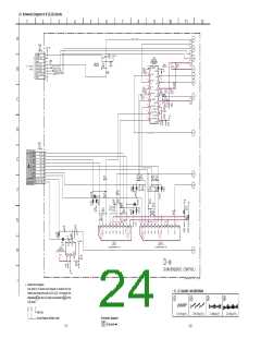
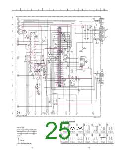
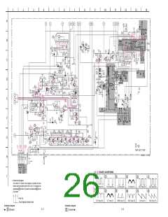
Note:
•
All capacitors are in µF unless otherwise noted. (pF: µµF)
Capacitors without voltage indication are all 50 V.
Indication of resistance, which does not have one for rating
electrical power, is as follows.
•
a
b
1
Ref. No.
Pitch: 5 mm
Circuit diagram division code
Rating electrical power 1/4 W (CHIP : 1/10 W)
•
All resistors are in ohms.
• f : nonflammable resistor.
• F : fusible resistor.
Terminal name of semiconductors in silk screen
printed circuit (
•
¢
: internal component.
A
)
• p : panel designation, and adjustment for repair.
H
*
•
All variable and adjustable resistors have characteristic curve B,
unless otherwise noted.
Circuit
Device
Printed symbol
Terminal name
Collector
Transistor
1
•
•
•
•
•
•
e
E
: earth-ground.
: earth-chassis.
Emitter
Collector
Emitter
Base
Transistor
Diode
All voltages are in V.
2
3
Base
Readings are taken with a 10 MΩ digital multimeter.
Readings are taken with a color-bar signal input.
Voltage variations may be noted due to normal production
tolerances.
Cathode
Anode
D
Cathode
4
5
6
7
8
Diode
Diode
Diode
Diode
(NC)
•
•
: Can not be measured.
Anode
*
Circled numbers are waveform references.
Cathode
• s : B + bus.
• S : B – bus.
(NC)
Anode
Common
•
The components identified by [ in this basic schematic diagram
have been carefully factory-selected for each set in order to
satisfy regulations regarding X-ray radiation.
Anode Cathode
Common
Anode Cathode
Common
Should replacement be required, replace only with the value
originally used.
Diode
Diode
Diode
•
•
When replacing components identified by ], make the
necessary adjustments indicated. (See page 3-1)
When replacing the part in below table, be sure to perform the
related adjustment.
Anode
Common
Anode
9
0
Anode Anode
Common
Cathode
Cathode
Part Replaced ([)
Common
!¡ Diode
HV ADJ
RV501
Cathode
Cathode
Anode
Anode
Cathode
Cathode
Anode
Anode
Diode
!™
Part Replaced (])
Source
Gate
Transistor
(FET)
Drain
Drain
!£
!¢
!∞
D
D
S
HV Regulator
Circuit Check
D board IC501, C532, C534,
C539, C553, C554,
C555, C556, C558,
C561, R541, R542,
R544, R564, R567,
R568, RV501,
G
G
Source
Gate
Transistor
(FET)
S
D
D
Source
Drain
Gate
Transistor
(FET)
G
G
S
S
Emitter
Collector
Base
Transistor
!§
T501 (FBT)
Discrete semiconductot
–
Ver.1.6
(Chip semiconductors that are not actually used are included.)
HV Protector
Circuit Check
D board IC607, IC901, D515,
D517, C540, C542,
C544, R510, R543
R547, R549, R552,
R595,
Note: The components identified by shading and mark
! are critical for safety. Replace only with part
number specified.
T501 (FBT)
Beam Current
Protector Circuit
Check
D board IC605, IC607, IC901,
C535, C541, R545,
R546, R548, R550,
R596, R934,
T501 (FBT)
5-5
5-6

 ETC [ ETC ]