MT88L70
Data Sheet
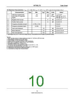
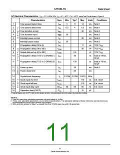
AC Electrical Characteristics - VDD = 3.0 V+20%/-10%, VSS = 0 V, -40°C ≤ To ≤ +85°C, using Test Circuit shown in Figure 6.
Characteristics
Sym.
Min.
Typ.‡
Max.
Units
Conditions
1
2
Tone present detect time
Tone absent detect time
Tone duration accept
tDP
tDA
5
11
4
14
8.5
40
ms Note 1
ms Note 1
ms Note 2
ms Note 2
ms Note 2
ms Note 2
0.5
T
I
3
tREC
tREC
tID
M
I
4
Tone duration reject
20
20
N
G
5
Interdigit pause accept
40
6
Interdigit pause reject
tDO
7
Propagation delay (St to Q)
Propagation delay (St to StD)
Output data set up (Q to StD)
Propagation delay (TOE to Q ENABLE)
tPQ
11
20
µs
µs
µs
TOE=VDD
8
O
U
T
tPStD
tQStD
tPTE
TOE=VDD
TOE=VDD
9
5.0
50
P
U
T
10
ns
load of 10 kΩ,
50 pF
S
11
Propagation delay (TOE to Q DISABLE)
tPTD
130
ns
load of 10 kΩ,
50 pF
P
D
W
N
12
13
Power-up time
tPU
tPD
30
20
ms Note 3
ms
Power-down time
14
15
16
17
18
Crystal/clock frequency
Clock input rise time
Clock input fall time
fC
3.5759 3.5795 3.5831 MHz
C
L
O
C
K
tLHCL
tHLCL
DCCL
CLO
110
110
60
ns
ns
%
Ext. clock
Ext. clock
Ext. clock
Clock input duty cycle
Capacitive load (OSC2)
40
50
15
pF
‡ Typical figures are at 25°C and are for design aid only: not guaranteed and not subject to production testing.
*NOTES:
1. Used for guard-time calculation purposes only and tested at -4 dBm.
2. These, user adjustable parameters, are not device specifications. The adjustable settings of these minimums and maximums are
recommendations based upon network requirements.
3. With valid tone present at input, tPU equals time from PDWN going low until ESt going high.
11
Zarlink Semiconductor Inc.

 ZARLINK [ ZARLINK SEMICONDUCTOR INC ]