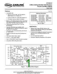
MT88E45
Data Sheet
1
2
3
4
5
6
7
8
9
10
20
IN2+
IN2-
GS2
CB2
VREF
IN1+
MT88E45B
19
18
17
16
15
14
13
12
11
IN1-
GS1
Vss
OSC1
OSC2
CB0
CB1
Vdd
CD
ST/GT
EST
DCLK
DATA
DR/STD
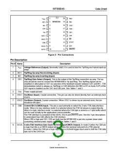
Figure 2 - Pin Connections
Pin Description
Pin # Name
Description
1
VREF Voltage Reference (Output). Nominally Vdd/2. It is used to bias the Tip/Ring and Hybrid input op-
amps.
2
3
4
IN1+ Tip/Ring Op-amp Non-inverting (Input).
IN1- Tip/Ring Op-amp Inverting (Input).
GS1 Tip/Ring Gain Select (Output). This is the output of the Tip/Ring connection op-amp. The op-
amp should be used to connect the MT88E45B to Tip and Ring. The Tip/Ring signal can be
amplified or attenuated at GS1 via selection of the feedback resistor between GS1 and IN1-. FSK
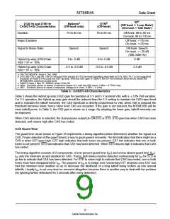
demodulation (which is always on Tip/Ring) or CAS detection (for MEI or BT on-hook CLIP) of the
GS1 signal is enabled via the CB1 and CB2 pins. See Tables 1 and 2.
5
6
Vss Power supply ground.
OSC1 Oscillator (Input). Crystal connection. This pin can also be driven directly from an external clock
source.
7
8
OSC2 Oscillator (Output). Crystal connection. When OSC1 is driven by an external clock, this pin
should be left open.
CB0 Control Bit 0 (CMOS Input). This pin is used primarily to select the 3-wire FSK data interface
mode. When it is low, interface mode 0 is selected where the FSK bit stream is output directly.
When it is high, interface mode 1 is selected where the FSK byte is stored in a 1 byte buffer which
can be read serially by the application’s microcontroller.
The FSK interface is consisted of the DATA, DCLK and DR/STD pins. See the 3 pin descriptions
to understand how CB0 affects the FSK interface.
When CB0 is high and CB1, CB2 are both low the MT88E45B is put into a power down state
consuming minimal power supply current. See Tables 1 and 2.
9
DCLK 3-wire FSK Interface Data Clock (Schmitt Input/CMOS Output). In mode 0 (when the CB0 pin
is logic low) this is a CMOS output which denotes the nominal mid-point of a FSK data bit.
In mode 1 (when the CB0 pin is logic high) this is a Schmitt trigger input used to shift the FSK data
byte out to the DATA pin.
3
Zarlink Semiconductor Inc.

 ZARLINK [ ZARLINK SEMICONDUCTOR INC ]