MT88E45
Data Sheet
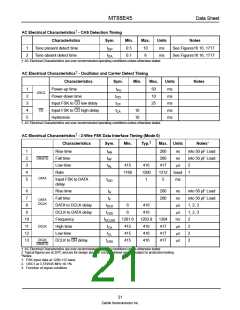
Word N+1
Word N
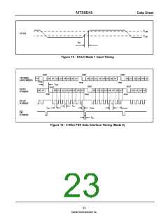
7
Demodulated Data
(Internal Signal)
1
5
stop
0
3
2
3
4
6
7
stop
tRL
start
Note 1
DR (Data Ready)
(Output)
Note 2
>tDDS
>tDDH
1/fDCLK1
DCLK (Data Clock)
(Schmitt Input)
DATA
(Output)
7
stop
0
1
2
4
5
6
7
stop
0
Word N-1
Word N
The DCLK input must be low before and after DR falling edge.
Note 1: DCLK occurs during DR low and returns DR to high.
Note 2: DCLK occurs after DR, so DR is low for half a nominal bit time.
Figure 14 - 3-Wire FSK Data Interface Timing (Mode 1)
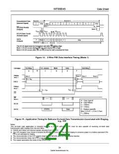
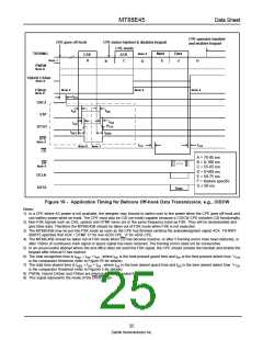
1st Ring
A
Ch. seizure
C
Data
E
2nd Ring
Note 2
Mark
D
TIP/RING
B
F
PWDN
Note 1
Note 2
tPU
Note 4
Note 3
tPD
OSC2
FSKen
Note 1
tCA
tCP
CD
DR
Note 5
A = 2sec typical
B = 250-500ms
C = 250ms
DCLK
DATA
D = 150ms
E = feature specific
..101010..
Data
Max C+D+E = 2.9 to 3.7sec
F ≥ 200ms
Figure 15 - Application Timing for Bellcore On-hook Data Transmission Associated with Ringing,
e.g., CID
Notes:
This on-hook case application is included because a CIDCW (off-hook) CPE must be also capable of receiving on-hook data
transmission (with ringing) from the end office.
1) PWDN and FSKen are internal signals decoded from CB0/1/2.
2) The CPE designer may choose to enable the MT88E45B only after the end of ringing to conserve power in a battery operated CPE.
CD is not activated by ringing.
3) The microcontroller in the CPE powers down the MT88E45B after CD has become inactive.
4) The microcontroller times out if CD is not activated.
5) This signal represents the mode of the DR/STD pin.
24
Zarlink Semiconductor Inc.

 ZARLINK [ ZARLINK SEMICONDUCTOR INC ]