MT88E43B
Data Sheet
MT88E43
VDD
C
VD=diode forward voltage
St/GT
ESt
R1
R2
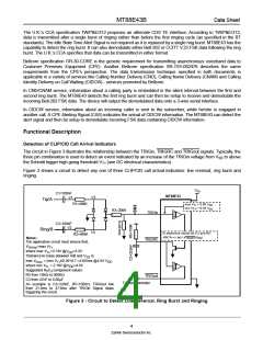
(a) tGP > tGA
tGP = R1C ln [VDD/(VDD-VTGt)]
tGA = RPC ln [(VDD-VD(RP/R2))/(VTGt-VD(RP/R2))]
RP = R1R2/(R1+R2)
MT88E43
VDD
C
VD=diode forward voltage
St/GT
R1
R2
ESt
(b) tGP < tGA
tGP = RPC ln [VDD-VD(RP/R2))/(VDD-VTGt-VD(RP/R2))]
tGA = R1C ln (VDD/VTGt
)
RP = R1R2/(R1+R2)
Figure 5 - Guard Time Circuits with Unequal Times
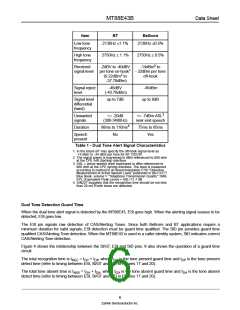
Input Configuration
The MT88E43 provides an input arrangement comprised of an operational amplifier and a bias source (VRef); which
is used to bias the opamp inputs at VDD/2. The feedback resistor at the opamp output (GS) can be used to adjust
the gain. In a single-ended configuration, the opamp is connected as shown in Figure 6. For a differential input
configuration, Figure 7 shows the necessary connections.
IN+
IN-
R
C
IN
GS
R
F
VRef
Voltage Gain
(A ) = R / R
IN
V
F
Figure 6 - Single-Ended Input Configuration
8
Zarlink Semiconductor Inc.

 ZARLINK [ ZARLINK SEMICONDUCTOR INC ]