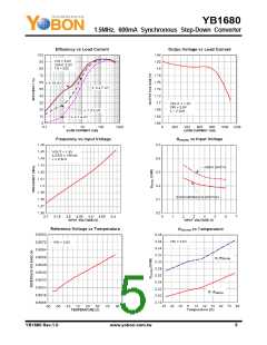
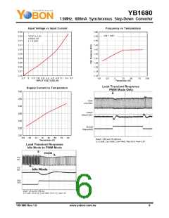
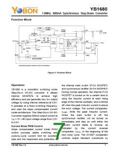
YB1680
1.5MHz, 600mA Synchronous Step-Down Converter
Absolute Maximum Ratings
Input Supply Voltage................... -0.3V to 6V Operating Temperature Range.. -40°C to 85°C
EN, VFB Voltage ................ -0.3V to VIN+0.3V Junction Temperature....................... 125°C
SW, VOUT Voltage.............. -0.3V to VIN+0.3V Storage Temperature Range ...-65°C to 150°C
Peak SW Sink and Source Current........1.5A Lead Temperature (Soldering, 10s) .. 300°C
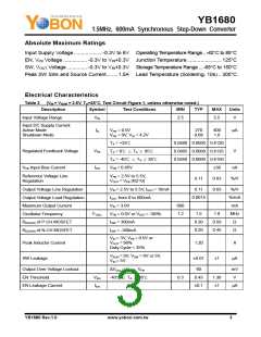
Electrical Characteristics
Table 2
(VIN = VRUN = 3.6V, TA=25°C, Test Circuit Figure 1, unless otherwise noted.)
Description
Symbol
Test Conditions
MIN
TYP
MAX
Units
Input Voltage Range
VIN
2.5
5.5
V
Input DC Supply Current
Active Mode
Shutdown Mode
IQ
V
V
FB = 0.5V
FB = 0V, VIN = 4.2V
270
0.08
400
1.0
μA
TA = +25℃
0.5880 0.6000 0.6120
0.5865 0.6000 0.6135
0.5850 0.6000 0.6150
±30
Regulated Feedback Voltage
VFB
V
TA = 0℃ ≦ TA ≦ 85℃
TA = -40℃ ≦ TA ≦ 85℃
VFB Input Bias Current
IFB
VFB = 0.65V
nA
Reference Voltage Line
Regulation
V
V
FB = 2.5V to 5.5V,
OUT = VFB (R2=0)
0.11
0.63
0.63
%/V
Output Voltage Line Regulation
Output Voltage Load Regulation
Maximum Output Current
Oscillator Frequency
VIN = 2.5V to 5.5V, IOUT = 10mA
IOUT from 0 to 600mA
VIN = 3.0V
0.11
%/V
%/mA
mA
MHz
Ω
0.0015
600
1.2
FOSC
VFB = 0.6V or VOUT = 100%
1.5
1.8
RDS(ON) of P-CH MOSFET
RDS(ON) of N-CH MOSFET
ISW = 300mA
0.30
0.20
0.50
0.45
ISW = -300mA
Ω
VIN = 3V, VFB = 0.5V or
Peak Inductor Current
SW Leakage
V
OUT = 90%
1.20
A
Duty Cycle < 35%
VRUN = 0V, VSW = 0V or 5V,
VIN = 5V
±0.01
±1
μA
Output Over Voltage Lockout
EN Threshold
ΔVOVL = VOVL - VFB
60
mV
V
VEN
IEN
-40℃ ≦ TA ≦ 85℃
0.3
0.45
±0.1
1.30
±1
EN Leakage Current
μA
YB1680 Rev.1.0
www.yobon.com.tw
3

 YOBON [ YOBON TECHNOLOGIES,INC. ]