XLSEMI 深圳市
科技有限公司
0755-83088967 83088481 Datasheet
3A 52KHz 40V Buck DC to DC Converter
XL2576
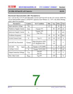
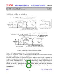
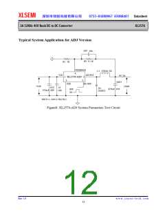
Test Circuit and Layout guidelines
LOCATE THE PROGRAMMING RESISTORS NEAR
THE FEEDBACK PIN USING SHORT LEADS
CFF
R2
KEEP FEEDBACK WIRING AWAY
FROM INDUCTOR FLUX
L1
R1 1K
FEEDBACK
4
REGULATED OUTPUT
VIN
OUTPUT
XL2576
1
2
ADJUSTABLE
3
5
GND
ON/OFF
UNREGULATED
DC INPUT
LOAD
CIN
C1
105
D1
COUT
OFF
ON
HEAVY LINES MUST BE KEPT SHORT AND USE
GROUND PLANE CONSTRUCTION FOR BEST RESULTS
VOUT=1.23*(1+R2/R1)
Figure5. Standard Test Circuits and Layout Guides
Select R1 to be approximately 1K, use a 1% resistor for best stability.
C1 and CFF are optional; in order to increase stability and reduce the input power line noise, CIN
and C1 must be placed near to PIN1 and PIN3;
For output voltages greater than approximately 10V, an additional capacitor CFF is required. The
compensation capacitor is typically between 100 pf and 33 nf, and is wired in parallel with the
output voltage setting resistor, R2. It provides additional stability for high output voltage, low
input-output voltages, and/or very low ESR output capacitors, such as solid tantalum capacitors.
CFF=1/(31*1000*R2); This capacitor type can be ceramic, plastic, silver mica, etc. (Because of
the unstable characteristics of ceramic capacitors made with Z5U material, they are not
recommended.)
Rev 1.0
w w w . j i n r u i - t e c h . c o m
8

 XILINX [ XILINX, INC ]