Spartan-3E FPGA Family: Pinout Descriptions
Material Declaration Data Sheets (MDDS) are also
available on the Xilinx web site for each package.
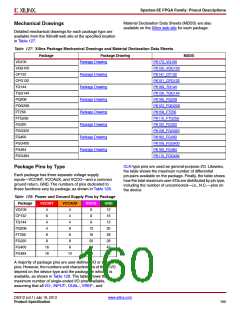
Mechanical Drawings
Detailed mechanical drawings for each package type are
available from the Xilinx® web site at the specified location
in Table 127.
Table 127: Xilinx Package Mechanical Drawings and Material Declaration Data Sheets
Package Package Drawing
Package Drawing
MDDS
VQ100
PK173_VQ100
PK130_VQG100
PK147_CP132
PK101_CPG132
PK169_TQ144
PK126_TQG144
PK166_PQ208
PK123_PQG208
PK158_FT256
PK115_FTG256
PK152_FG320
PK106_FGG320
PK182_FG400
PK108_FGG400
PK183_FG484
PK110_FGG484
VQG100
CP132
Package Drawing
Package Drawing
Package Drawing
Package Drawing
Package Drawing
Package Drawing
Package Drawing
CPG132
TQ144
TQG144
PQ208
PQG208
FT256
FTG256
FG320
FGG320
FG400
FGG400
FG484
FGG484
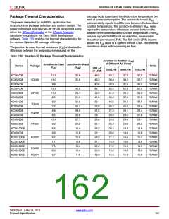
CLK-type pins are used as general-purpose I/O. Likewise,
the table shows the maximum number of differential
pin-pairs available on the package. Finally, the table shows
how the total maximum user-I/Os are distributed by pin type,
including the number of unconnected—i.e., N.C.—pins on
the device.
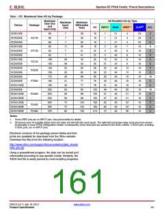
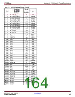
Package Pins by Type
Each package has three separate voltage supply
inputs—VCCINT, VCCAUX, and VCCO—and a common
ground return, GND. The numbers of pins dedicated to
these functions vary by package, as shown in Table 128.
Table 128: Power and Ground Supply Pins by Package
Package
VQ100
CP132
TQ144
PQ208
FT256
VCCINT
VCCAUX
VCCO
8
GND
12
4
6
4
4
8
16
4
4
9
13
4
8
12
16
20
24
28
20
8
8
28
FG320
FG400
FG484
8
8
28
16
16
8
42
10
48
A majority of package pins are user-defined I/O or input
pins. However, the numbers and characteristics of these I/O
depend on the device type and the package in which it is
available, as shown in Table 129. The table shows the
maximum number of single-ended I/O pins available,
assuming that all I/O-, INPUT-, DUAL-, VREF-, and
DS312 (v4.1) July 19, 2013
www.xilinx.com
Product Specification
160

 XILINX [ XILINX, INC ]