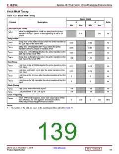
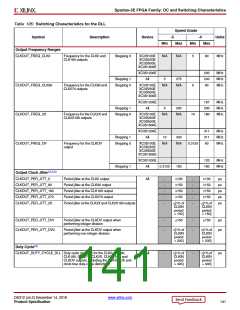
Spartan-3E FPGA Family: DC and Switching Characteristics
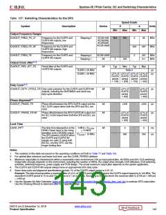
Table 107: Switching Characteristics for the DFS
Speed Grade
Symbol
Description
Device
-5
-4
Units
Min
Max
Min
Max
Output Frequency Ranges
CLKOUT_FREQ_FX_LF
Frequency for the CLKFX and
CLKFX180 outputs, low
frequencies
Stepping 0
XC3S100E
XC3S250E
XC3S500E
XC3S1600E
N/A
N/A
5
90
MHz
MHz
CLKOUT_FREQ_FX_HF
CLKOUT_FREQ_FX
Frequency for the CLKFX and
CLKFX180 outputs, high
frequencies
220
5
307
Frequency for the CLKFX and
CLKFX180 outputs
Stepping 0
Stepping 1
XC3S1200E
All
307
311
MHz
MHz
5
333
Output Clock Jitter(2,3)
CLKOUT_PER_JITT_FX
Period jitter at the CLKFX and
CLKFX180 outputs.
All
All
Typ
Max
Typ
Max
CLKIN ≤ 20 MHz
CLKIN > 20 MHz
Note 6
ps
ps
[1% of [1% of [1%of [1%of
CLKFX CLKFX CLKFX CLKFX
period period period period
+ 100] + 200] + 100] + 200]
Duty Cycle(4,5)
CLKOUT_DUTY_CYCLE_FX Duty cycle precision for the CLKFX and CLKFX180
outputs, including the BUFGMUX and clock tree
duty-cycle distortion
-
[1% of
CLKFX
period
+ 400]
-
[1%of
CLKFX
period
+ 400]
ps
Phase Alignment(5)
CLKOUT_PHASE_FX
Phase offset between the DFS CLKFX output and the
DLL CLK0 output when both the DFS and DLL are
used
All
All
-
-
200
-
-
200
ps
ps
CLKOUT_PHASE_FX180
Phase offset between the DFS CLKFX180 output and
the DLL CLK0 output when both the DFS and DLL are
used
[1% of
CLKFX
period
+ 300]
[1%of
CLKFX
period
+ 300]
Lock Time
(2)
LOCK_FX
The time from deassertion at the
DCM’s Reset input to the rising
transition at its LOCKED output.
The DFS asserts LOCKED when
the CLKFX and CLKFX180
signals are valid. If using both
the DLL and the DFS, use the
longer locking time.
5 MHz ≤ F
All
-
-
5
-
-
5
ms
CLKIN
≤ 15 MHz
F
> 15 MHz
450
450
μs
CLKIN
Notes:
1. The numbers in this table are based on the operating conditions set forth in Table 77 and Table 106.
2. For optimal jitter tolerance and faster lock time, use the CLKIN_PERIOD attribute.
3. Maximum output jitter is characterized within a reasonable noise environment (150 ps input period jitter, 40 SSOs and 25% CLB switching).
Output jitter strongly depends on the environment, including the number of SSOs, the output drive strength, CLB utilization, CLB switching
activities, switching frequency, power supply and PCB design. The actual maximum output jitter depends on the system application.
4. The CLKFX and CLKFX180 outputs always have an approximate 50% duty cycle.
5. Some duty-cycle and alignment specifications include 1% of the CLKFX output period or 0.01 UI.
Example: The data sheet specifies a maximum jitter of [1% of CLKFX period + 300]. Assume the CLKFX output frequency is 100 MHz. The
equivalent CLKFX period is 10 ns and 1% of 10 ns is 0.1 ns or 100 ps. According to the data sheet, the maximum jitter is [100 ps + 300 ps]
=
400 ps.
6. Use the Spartan-3A Jitter Calculator (www.xilinx.com/support/documentation/data_sheets/s3a_jitter_calc.zip) to estimate DFS output jitter.
Use the Clocking Wizard to determine jitter for a specific design.
DS312 (v4.2) December 14, 2018
www.xilinx.com
Product Specification
143

 XILINX [ XILINX, INC ]