R
Pinout Descriptions
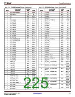
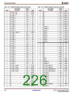
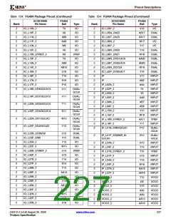
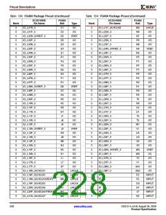
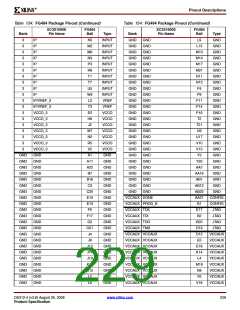
Table 154: FG484 Package Pinout (Continued)
Table 154: FG484 Package Pinout (Continued)
XC3S1600E
Pin Name
FG484
Ball
XC3S1600E
Pin Name
FG484
Ball
Bank
Type
Bank
Type
VCCAUX VCCAUX
VCCINT VCCINT
VCCINT VCCINT
VCCINT VCCINT
VCCINT VCCINT
VCCINT VCCINT
VCCINT VCCINT
VCCINT VCCINT
VCCINT VCCINT
VCCINT VCCINT
W11
J10
K9
VCCAUX
VCCINT
VCCINT
VCCINT
VCCINT
VCCINT
VCCINT
VCCINT
VCCINT
VCCINT
VCCINT VCCINT
VCCINT VCCINT
VCCINT VCCINT
VCCINT VCCINT
VCCINT VCCINT
VCCINT VCCINT
VCCINT VCCINT
M11
M12
M13
N10
N12
N14
P13
VCCINT
VCCINT
VCCINT
VCCINT
VCCINT
VCCINT
VCCINT
K11
K13
L10
L11
L12
L14
M9
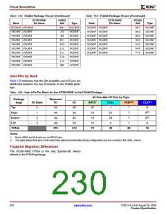
User I/Os by Bank
Table 155 indicates how the 304 available user-I/O pins are
distributed between the four I/O banks on the FG484 pack-
age.
Table 155: User I/Os Per Bank for the XC3S1600E in the FG484 Package
All Possible I/O Pins by Type
Package
Edge
Maximum
I/O
(1)
(1)
I/O Bank
I/O
56
INPUT
DUAL
1
VREF
CLK
Top
0
1
2
3
94
94
22
16
18
16
72
7
7
8
(2)
Right
50
21
24
0
0
(2)
Bottom
Left
94
45
7
0
94
63
7
8
TOTAL
376
214
46
28
16
Notes:
1. Some VREF and CLK pins are on INPUT pins.
2. The eight global clock pins in this bank have optional functionality during configuration and are counted in the DUAL column.
Footprint Migration Differences
The XC3S1600E FPGA is the only Spartan-3E device
offered in the FG484 package.
230
www.xilinx.com
DS312-4 (v3.8) August 26, 2009
Product Specification

 XILINX [ XILINX, INC ]